
What Is EMI Shielding?
Struggling with failed EMC tests, mysterious signal noise, or gasket failures in the field? EMI shielding — using conductive materials to block unwanted electromagnetic interference — is often where the problem starts, and where the fix lives.
Over hundreds of enclosure shielding projects, we’ve seen the same two numbers separate reliable products from costly recalls: a 93–98% groove fill ratio and 15–25% gasket compression. Get these right, and most EMI headaches disappear.
In this guide, you’ll learn the four core shielding materials, field-tested design rules, a 6-step FIP selection framework, and a ready-to-use checklist — everything you need to design EMI shielding that passes the first time. Let’s dive in.
Why EMI Shielding Is Critical in Modern Electronics
EMI shielding used to be an afterthought. Today, it’s a gating factor for whether your product ships at all.
Every market demands EMC certification. Selling globally means passing FCC (US), CE (EU), VCCI (Japan), 3C (China), and C-TICK / RCM (Australia). One failed scan can push your launch back by 3–6 months — and re-spinning an enclosure after tooling is locked is where budgets quietly die.
Mission-critical applications leave zero margin for error. 5G base stations operate at mmWave frequencies where a 1 mm shielding gap leaks measurable power. Automotive ADAS radar at 24 GHz and 77 GHz must distinguish a pedestrian from a guardrail — EMI noise here isn’t a compliance issue, it’s a safety issue. Medical imaging, avionics, and defense systems face the same reality.
The cost of ignoring EMI compounds fast: failed certification → tooling rework → product recalls → field warranty claims → brand damage. We’ve seen a single overlooked gasket groove cost a client over $400K in re-certification and delayed shipments.
The key principle: EMI shielding must be designed in at the concept stage, alongside thermal and mechanical design — never bolted on after the enclosure is finalized.

How EMI Shielding Works
EMI shielding works through two physical mechanisms — and understanding both is the difference between specifying the right material and over-engineering the wrong one.
Reflection happens when electromagnetic waves hit a conductive surface (aluminum, copper, silver-filled elastomers) and bounce back, much like light off a mirror. This handles most low-to-mid frequency interference.
Absorption happens when lossy materials — ferrites, carbon-loaded foams, nickel-coated fibers — convert EM energy into tiny amounts of heat. This dominates at higher frequencies and inside resonant cavities.
But here’s what most designers miss: shielding only works if the conductive path is continuous and properly grounded. A shielded enclosure with one ungrounded seam behaves like a bucket with a hole — the leak defines the performance, not the material.
Frequency math makes this brutal. At 10 GHz, the wavelength is just 30 mm. A 1 mm slot acts like a slot antenna, radiating EMI straight out. This is exactly why gaskets, FIP seals, and conductive coatings exist — to close those millimeter-scale gaps that PCB shields and metal enclosures alone cannot.
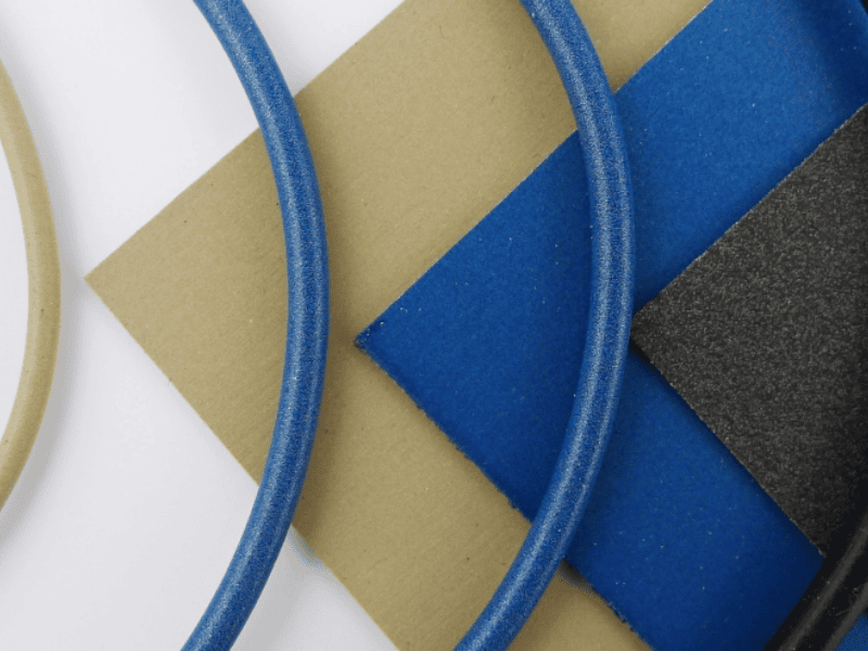
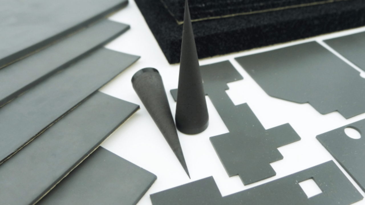
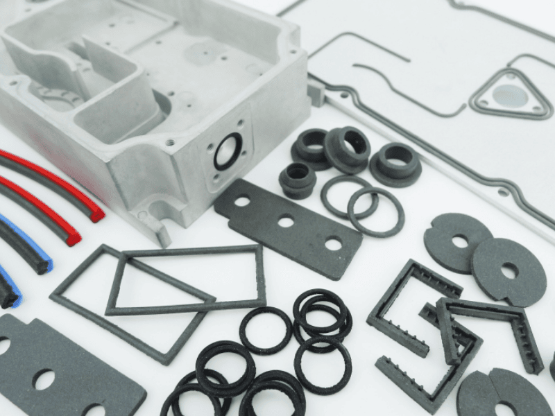
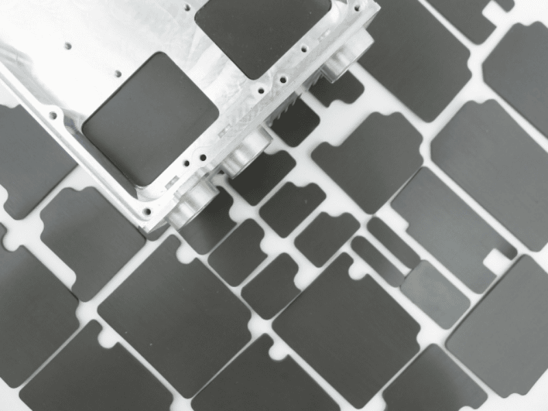
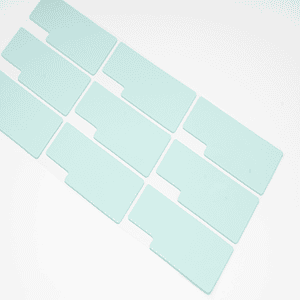
Core EMI Shielding Materials Overview
There is no “best” EMI shielding material — only the right material for your geometry, frequency, environment, and budget. Most failed designs we’ve reviewed used the right material in the wrong application. Here are the four families that cover 95% of real-world projects.
🔹 Four Material Families at a Glance
| Material Type | Best For | Typical Applications | Form Factor |
|---|---|---|---|
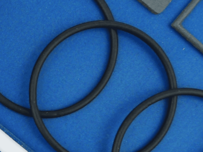
| Conductive Elastomers (silicone-based) | Sealing + shielding in one part | Enclosure gaskets, lids, covers, military housings | Molded / extruded |
| Form-In-Place (FIP) Adhesives | Complex geometries, narrow grooves (≥0.5 mm) | Optical modules, 5G RF housings, base stations | Robot-dispensed |
| EMI Absorbers | Reducing cavity resonance & antenna coupling | Radar, mmWave, ADAS, high-speed PCBs | Sheet / paste |
| Conductive Foams & Fabrics | Lightweight, flexible, low-compression shielding | Consumer electronics, displays, laptops | Die-cut / wrapped |
💡 Quick decision rule: Need a seal + shield in one? → Elastomer. Groove too narrow to mold? → FIP. Fighting resonance, not leakage? → Absorber. Just need low-cost shielding? → Foam/fabric.
🔹 Filler Chemistry Determines Performance
Shielding effectiveness, corrosion resistance, and cost are all driven by the conductive filler inside the elastomer or adhesive — not the base polymer.
| Filler System | Shielding (typical) | Key Strength | Trade-off |
|---|---|---|---|
| Silver / Copper (Ag/Cu) | >100 dB | Highest performance | Premium cost, copper oxidation risk |
| Silver / Aluminum (Ag/Al) | ~100 dB | Excellent corrosion resistance, lightweight | Higher cost than Ni-based |
| Silver / Nickel (Ag/Ni) | ~90–100 dB | Balanced performance + cost | Mid-tier price |
| Nickel / Graphite (Ni/C) | >80 dB | Cost-effective workhorse | Lower performance ceiling |
Rule of thumb: Don’t pay for Ag/Cu if Ni/C meets your spec. Don’t save on Ni/C if you’re shielding a 77 GHz radar.

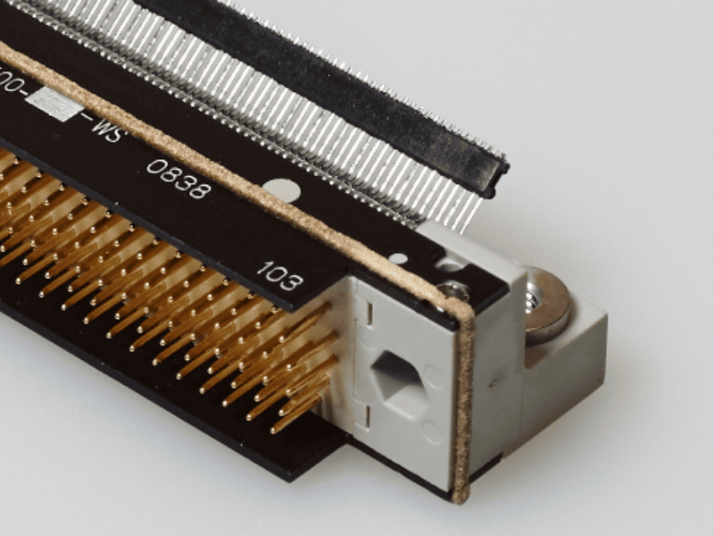
EMI Gasket Design Essentials
Field Engineering Rules That Separate Reliable Designs from Field Failures
After working on hundreds of enclosure shielding projects, experienced engineers consistently apply these proven numbers:
✅ Groove fill ratio: 93%–98% — Under-filling creates EMI leak paths; over-filling damages the gasket and prevents proper enclosure closure
✅ Compression deformation: 15%–25% for solid profiles — Below 10% loses electrical contact; above 25% accelerates compression set and shortens lifespan
✅ Use hollow O-shaped or D-shaped profiles for thin-walled enclosures — they achieve the required compression with significantly lower closure force
✅ Verify electrochemical compatibility between the gasket filler and the mating metal surface — for example, silver-based gaskets paired with bare aluminum in humid environments will trigger galvanic corrosion, causing contact resistance to rise and shielding effectiveness to collapse within months
Why these rules matter: These specific parameters are rarely discussed in vendor brochures but are exactly where most EMI shielding designs fail in production.

Form-In-Place (FIP) Gaskets: When Standard Gaskets Aren’t Enough
When extruded or molded gaskets hit their physical limits — too narrow, too complex, too high-volume — Form-In-Place (FIP) is the answer. FIP is a robotic dispensing process that lays conductive adhesive directly onto the substrate, curing into a custom gasket bonded exactly where you need it.
🔹 When to Choose FIP Over Standard Gaskets
| Trigger | Why FIP Wins |
|---|---|
| Grooves as narrow as 0.3 mm | Impossible to extrude or hand-place |
| Complex 3D geometry (steps, corners, multi-plane paths) | Molded gaskets can’t follow; FIP robots can |
| High-volume automation required | Robotic dispensing scales without labor cost |
| Mixed-height sealing surfaces | Bead height adjusts dynamically |
If your design hits any one of these triggers, FIP is no longer optional — it’s the only manufacturable solution.

💡 A 6-Step Framework for Selecting the Right FIP Conductive Adhesive
The wrong FIP choice leads to bead collapse, poor adhesion, or shielding failure in the field. Apply these six checks — in order — before specifying any FIP material:
Step 1 — Define the Shielding Effectiveness (SE) Target
- >100 dB → Ag/Cu or Ag/Al (mmWave, radar, defense)
- 80–100 dB → Ag/Ni (5G base stations, telecom)
- >80 dB at lowest cost → Ni/C (industrial, consumer electronics)
Step 2 — Match Cure Profile to Substrate Heat Tolerance
- RTV (room-temperature cure) → heat-sensitive PCBs, plastics, pre-assembled modules
- Heat-cure → bare metal housings on automated lines (faster cycle, stronger adhesion)
- ⚠️ Curing an RTV adhesive on a hot substrate, or heat-curing on a plastic carrier, is the #1 cause of bead defects in new FIP lines
Step 3 — Stress-Test Against the Operating Environment
- Coastal / humid / salt-spray → Ag/Al (corrosion-resistant)
- Indoor industrial → Ni/C acceptable
- Outdoor telecom (–40°C to +85°C) → verify both filler stability AND elastomer compression set
Step 4 — Specify Cured Hardness (Shore A)
Hardness determines required closure force and screw torque density — a hard bead in a thin-wall enclosure will warp the lid before it seals.
- Typical FIP range: Shore A 35–65
- Thin-wall / lightweight housings → softer (35–45)
- Heavy aerospace / military lids → harder (55–65)
Step 5 — Validate Bead Dimensions
| Bead Geometry | Specification |
|---|---|
| Minimum bead width | 0.3 mm |
| Recommended (best yield + reliability) | 1.0 mm W × 0.73 mm H |
| Maximum bead | 2.5 mm W × 1.7 mm H |
Step 6 — Optimize Cost Against Actual SE Requirement
- Don’t pay for Ag/Cu when Ni/C meets spec — the cost gap can exceed 5–8×
- Don’t save on Ni/C if you’re shielding 77 GHz radar — one field failure costs more than a lifetime of Ag/Cu
⚠️ Common Pitfall: Know When FIP Stops Being the Right Tool
When groove width exceeds 2.5 mm, FIP becomes inefficient — dispensing time, material cost, and bead-shape stability all degrade. Switch to extruded conductive rubber strips instead. Using FIP outside its sweet spot is one of the most expensive specification errors we see in industry.
EMI Absorber Materials: Solving What Shielding Alone Can’t
Conductive shielding reflects EMI energy. In open space, that’s fine — the energy bounces away. But inside a tight metal enclosure, that reflected energy has nowhere to go: it bounces between walls, builds standing waves, and re-couples into sensitive circuits as secondary interference.
Absorbers solve what shielding cannot — they convert EMI energy into heat through magnetic or dielectric loss, removing it from the system entirely.
🔹 When Absorbers Become Mandatory (Not Optional)
| Symptom | Root Cause | Absorber Role |
|---|---|---|
| Cavity resonance inside metal housings | Reflected waves form standing patterns | Damps resonant peaks |
| Antenna-to-antenna coupling in radar / MIMO | Direct + reflected paths interfere | Suppresses unwanted coupling |
| Self-interference in optical transceivers | High-speed signals radiate inside the shield | Absorbs near-field energy |
| ADAS radar crosstalk (24 / 77 GHz) | Multiple radar channels in one module | Isolates Tx/Rx paths |
🔹 Frequency Coverage of Modern Absorbers
| Frequency Range | Typical Application |
|---|---|
| MHz range | NFC, RFID, wireless charging |
| 1–18 GHz | Wi-Fi, 5G sub-6, telecom |
| 24 / 77 GHz | Automotive radar, ADAS |
| Up to 110 GHz | mmWave radar, satellite, 6G research |
💡 Best Practice: Shield + Absorb, Not Shield OR Absorb
In high-frequency systems above 10 GHz, the highest-performing designs combine both:
- Conductive gasket / FIP → blocks energy from entering or escaping
- Absorber sheet / paste → kills internal reflections before they cause harm
Used alone, each approach hits a ceiling. Used together, they deliver EMC margin that neither can achieve independently — which is why every production-grade 77 GHz radar module we’ve seen uses this dual-layer strategy.
EMI Shielding Effectiveness & Testing
A material is only as good as its measured performance — and in EMC, measurement methods can make a 20 dB difference for the same gasket. Understanding how SE is tested is as critical as knowing what value to target.
🔹 Shielding Effectiveness (SE) — What the Numbers Mean
| SE Range | Grade | Typical Applications |
|---|---|---|
| 30–60 dB | Basic shielding | Consumer electronics, indoor IoT |
| 60–90 dB | Commercial-grade | Telecom, industrial control, medical |
| 90+ dB | High-performance / mission-critical | Defense, aerospace, mmWave radar, secure communications |
SE is logarithmic: every 20 dB = 10× reduction in field strength. A jump from 60 to 80 dB is not “33% better” — it’s 10× better.
🔹 Key Testing Standards — Know Which Applies to You
| Standard | Scope | When to Cite It |
|---|---|---|
| MIL-DTL-83528C | Conductive elastomer SE testing | Gasket material qualification |
| ASTM D4935 | Planar material SE (1 MHz–1.5 GHz) | Conductive films, fabrics, sheet shielding |
| IEEE 299 | Enclosure-level SE (full system) | Verifying the actual finished product |
⚠️ Common procurement mistake: Accepting an ASTM D4935 material report as proof of enclosure performance. Material SE ≠ Enclosure SE. Always require IEEE 299 for system-level acceptance.
🔹 Three Test Dimensions You Should Specify
- Reflectivity — measured via arch reflectivity method, 1–110 GHz → Critical for absorbers and anechoic applications
- Attenuation / Insertion Loss — measured via free-space transmission → The number you actually care about for shielding performance
- Electromagnetic parameters (ε, μ) — measured via coaxial line method → Required for simulation, material development, and high-frequency design validation
⚠️ Engineering Tip: Above 18 GHz, Demand Full-Band Sweep
For mmWave applications (24 GHz ADAS, 77 GHz radar, 5G mmWave, 110 GHz research):
- Single-point compliance does NOT guarantee broadband performance
- Materials can show 90 dB at one spot frequency and collapse to 40 dB just 2 GHz away
- Always require full-band sweep data in the qualification report — not a 3-point summary
This single requirement filters out 70% of unqualified suppliers before you ever build a prototype.
EMI Shielding Material Selection Checklist
After 8 sections of theory, frameworks, and warnings — here is the one-page checklist you can take into your next design review. If any item is unchecked before tooling release, stop and resolve it. Every field failure we’ve debugged in 15 years traces back to a missed item on this list.
📋 The Pre-Design Checklist
✅ Performance Targets
- Shielding effectiveness target defined — specify both dB value AND frequency range (e.g., “>90 dB from 1 MHz to 40 GHz”)
- Operating temperature range confirmed — typical silicone range: –55°C to +170°C; fluorosilicone extends chemical resistance
- Environmental sealing specified — IP rating documented (e.g., IP68), including dust, water, and salt-spray if applicable
✅ Material & Compatibility
- Electrochemical compatibility validated — filler metal vs. mating flange metal checked against galvanic table (revisit Section 2)
- Corrosion-protection strategy defined if ΔV > 0.3 V — conductive coating, isolation layer, or filler change
✅ Mechanical Design
- Compression range designed at 15%–25% — never below 10%, never above 30%
- Groove fill ratio designed at 93%–98% — leaves room for thermal expansion, prevents bead extrusion
- Closure force budget matched to enclosure stiffness — soft gasket for thin-wall housings, harder for rigid lids
- Screw spacing ≤ 25 mm for high-SE applications (>80 dB)

✅ Manufacturing & Cost
- Gasket form factor selected — extruded / molded / FIP / fabric-over-foam — matched to groove geometry (revisit Section 6)
- Cost vs. performance balanced — no Ag/Cu where Ni/C meets spec; no Ni/C where mission-critical SE is required
- Test standards cited in spec sheet — MIL-DTL-83528C / ASTM D4935 / IEEE 299 (revisit Section 8)
- Full-band sweep test required if operating above 18 GHz
💡 How to use this checklist:Run it twice— once at concept-design stage (before CAD freeze), and again at DFM review (before tooling release). The second pass catches what the first one missed.
Final Thoughts: Designing EMI Shielding That Lasts
- EMI shielding success comes down to three fundamentals: the right material, the right geometry, and the right testing. Miss any one, and premium fillers won’t save the design.Engage shielding expertise early. A concept-stage design review costs a fraction of a late-stage redesign — and a tiny fraction of a field recall.When selecting a partner, prioritize suppliers who offer:
- ✅ In-house testing aligned to MIL / ASTM / IEC standards✅ Material selection consultation, not just a catalog✅ Rapid prototyping without expensive tooling✅ Documented performance data — full-band, not single-point

