
Looking for solutions to on-board charger (OBC) design challenges?
In this piece, we’ll explore the main ones. In an EV, the OBC is the circuit that converts AC power from the grid to DC for the battery while protecting components from high voltage and managing heat that can cripple performance or shorten lifespan.
This isn’t the first time EVs have taken the spotlight. Their first rise came in the late 1800s to early 1900s, but faded with the arrival of mass-produced internal combustion engine (ICE) vehicles and weak early batteries.
Over a century later, with advancements in technology and the development of smarter batteries, EVs are making a comeback, driven by automakers eager to dominate the market. Still, challenges remain. Companies such as Tesla are now racing to build smaller, more affordable electric cars in the $25,000–$30,000 range, competing directly with traditional hatchbacks. Around 15% of announced future U.S. EV models may fall into the medium-size category.
The problem stems from the drive for higher power density, which means more power in less space. Too much heat threatens reliability, and a limited surface area makes cooling complex. Add to that the need for high-voltage dielectric isolation, which demands careful spacing, insulation, and transformer design within already compact systems.
Let us explore how engineers are addressing these twin challenges in modern OBC design.
The Anatomy of an OBC
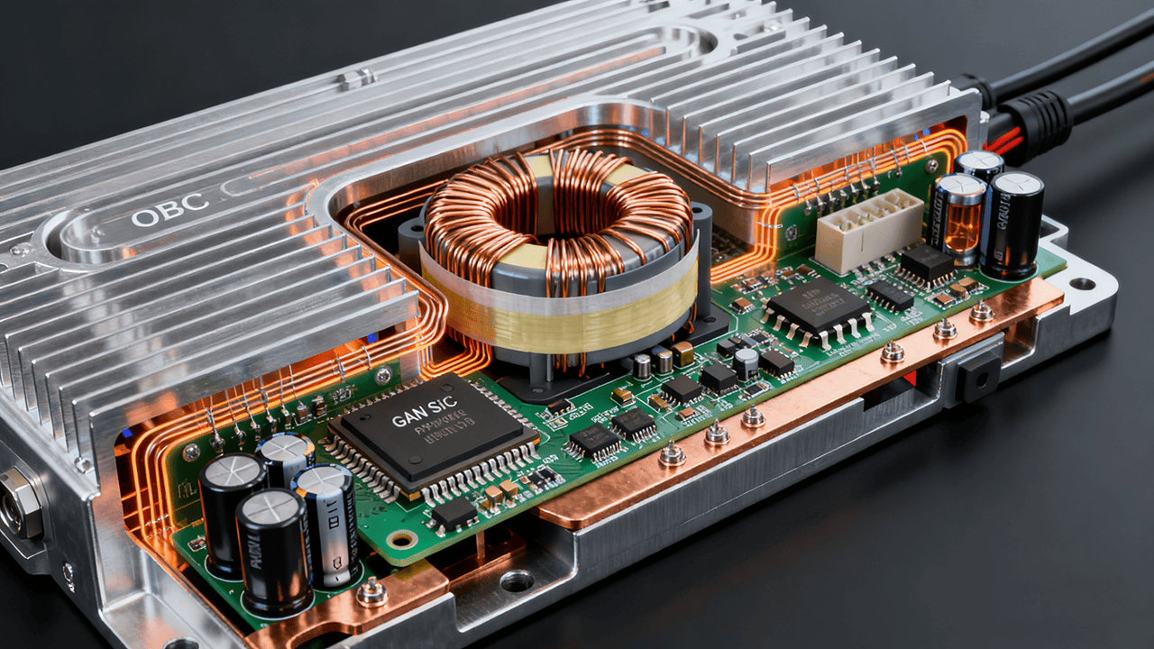
We want you to have a clear picture of what happens inside an on-board charger (OBC). This remarkable EV component sits between the power grid (AC) and the vehicle’s battery (DC), converting 120–240 V AC from a wall socket or station into 400–800 V DC for the battery while keeping the process safe and efficient. Level 1 charging, which is the slowest, uses a 120-volt outlet and adds about 4 miles of range per hour, while Level 2 charging uses a 240-volt outlet and adds around 20–25 miles per hour.
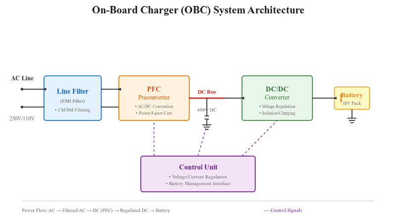
In today’s EVs, the OBC’s power flow typically involves three building blocks: the AC/DC converter, the DC/DC converter, and the high-frequency transformer. The AC/DC converter performs power factor correction (PFC) and rectifies AC to DC, targeting >95% efficiency with topologies such as bridgeless totem-pole or interleaved boost converters.
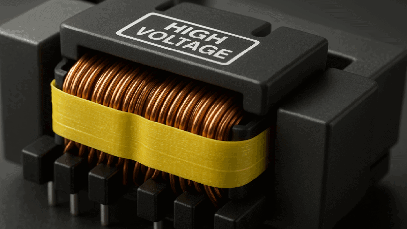
The DC/DC converter handles isolation and precise battery voltage control, converting 400–450 V DC from the previous stage to 400–800 V depending on the EV, while supporting CC/CV profiles with topologies such as DAB and LLC. Between these stages lies the high-frequency transformer, built with ferrite or nanocrystalline cores to provide galvanic isolation between grid and battery, operating at 100–300 kHz for compactness.
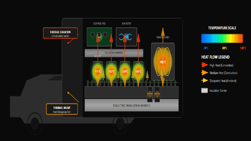
Heat mainly comes from semiconductor switching losses, magnetic core losses, and resistive copper losses. These are issues every OBC engineer must manage carefully.
Heat Dissipation Challenges
When we look inside an on-board charger (OBC), almost every critical component turns part of the input power into heat. During operation, semiconductors switch rapidly, transformers handle magnetic flux, and even copper traces resist current flow.
MOSFETs (Metal-Oxide-Semiconductor Field-Effect Transistors) and diodes flip on and off thousands of times per second (50–500 kHz), producing switching losses in semiconductors. The higher the switching frequency and voltage, the greater the energy lost as heat.
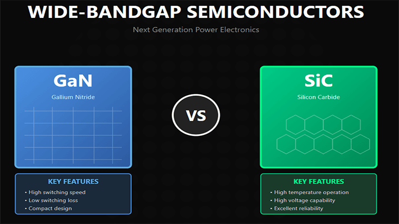
Although Gallium Nitride (GaN) and Silicon Carbide (SiC) reduce switching losses compared to silicon, concentrated hotspots still form. That is why, in GaN converter design, strategies including precise component placement and thermal vias are used to create efficient heat pathways that draw energy away from the device.
Core and copper losses in transformers and inductors are another notable source of heat. At higher frequencies, core losses (eddy current and hysteresis) rise, while copper losses result from current flow and the skin and proximity effects. This sometimes pushes magnetic component temperatures past 100 °C if cooling isn’t optimized.
As designers push for smaller, lighter OBCs, natural surface area for cooling decreases while power density (3–10 kW/L) remains high. Essentially, the same heat in a tighter compartment. This heat concentration can shorten component lifespan and threaten nearby control circuits.
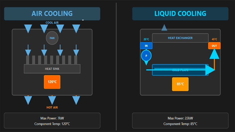
Traditionally, liquid or forced-air cooling is used. Liquid cooling works efficiently but adds weight, cost, and potential failure points such as pumps and seals. Air cooling, meanwhile, struggles with dense layouts. Some designs reuse the vehicle’s coolant loop, but that tightly couples OBC thermal behavior to the drivetrain system.
Wide-bandgap (WBG) devices such as SiC and GaN switch faster (200–500 kHz), boosting efficiency but concentrating heat into tiny chip areas. GaN switches faster than SiC, because of the higher electron mobility and lower capacitance. These high thermal gradients, sometimes over 30 °C within millimeters, stress solder joints and packaging materials.
Recent OBC research integrates heat management directly into the silicon package, using sintered silver, embedded dies, and graphene films to pull heat away almost as fast as it forms. Yet even efficient systems face silent wear: each charge cycle expands and contracts materials differently, gradually cracking solder joints and layers over time.
High-Voltage Dielectric Isolation Challenges

Dielectric or galvanic isolation is the process of separating two circuits, in this case, the high-voltage AC from the grid and the vehicle’s low-voltage DC battery system. This is so that the voltage from the high side never leaks to the low side. This protects both users and electronics from hazardous voltages and electrical noise through a dielectric material (an insulator) that enables energy transfer magnetically, not electrically.
Since an OBC connects 240 V AC (or higher in commercial EVs) to 400–800 V DC battery lines, the potential difference is enormous. Any isolation failure could result in electric shock, short circuits, or catastrophic battery damage.
Dielectric strength and isolation voltage determine isolation reliability.
- Dielectric strength refers to the insulating material’s inherent ability to resist breakdown,
- while isolation voltage is the tested system-level limit under defined safety standards.
Dielectric strength, measured in kV/mm or V/mil, represents the maximum electric field an insulator can endure before failure. It depends on factors such as composition, thickness, voltage duration, and humidity.
Isolation voltage (also called dielectric withstand voltage) is the highest voltage the system can sustain across its barrier for a short time. For instance, 3000 VAC for 60 seconds, without breakdown or excessive leakage. Meeting standards such as UL, IEC, or CE makes user safety certain even under transient or fault conditions.

In an OBC, the high-frequency transformer inside the DC/DC converter provides primary isolation, operating at 100–300 kHz. However, tighter spacing raises insulation stress, making creepage and clearance indispensable to prevent arcing or tracking.
Wider spacing and thicker insulation improve safety but worsen heat dissipation and increase size. To manage both insulation and heat, engineers now use nanocomposite insulation materials, polymers enhanced with thermally conductive nanofillers, that achieve higher thermal conductivity than pure polymers (e.g., polyimide, epoxy resin) while maintaining electrical strength.
As OBC voltages exceed 800 V, even microscopic voids can trigger partial discharges that erode insulation. To counter this, designs increasingly rely on vacuum potting and advanced encapsulation, which is to guarantee compliance with UL 62109, IEC 61800, and IEC 60664 standards, where most OBCs must withstand 2–4 kV isolation voltage during testing.
Balancing Thermal and Electrical Design
The matter is mind-boggling, with each improvement having the potential to hurt another. Thicker insulation makes it harder for heat to escape, while better cooling often compromises electrical spacing (creepage and clearance, both vital for high-voltage safety).
Some engineers mitigate this by using thermally conductive but electrically insulating pads, such as JIUJU’s 6X15 series, which might be suitable for situations where both high thermal conductivity and 10 kV dielectric strength are required.
In transformers, insulation meant for electrical protection also affects thermal management. The relationship is inverse: thicker insulation hinders airflow, raises thermal resistance, and accelerates degradation.
The headache in transformer design lies in balancing sufficient insulation thickness for electrical safety and efficient heat dissipation for reliability. Modern efforts focus on improving material properties instead of merely thinning insulation.
Efficient cooling systems (oil circulation, fans, or radiators) are valuable for removing heat while keeping insulation within safe limits. Adding insulation boosts dielectric strength but traps heat; adding metal cooling plates removes heat but shortens safety distances.
Dense layouts reduce parasitics but worsen thermal coupling between hot zones. This thermal-electrical coupling directly affects OBC performance, reliability, and lifespan.
Today, engineers model temperature and electric fields together using advanced PCB materials such as ceramic-filled FR4, aluminum nitride, and IMS boards. Dual-purpose potting compounds and integrated cooling loops, used by Hyundai and Tesla, now define the industry’s move toward shared, thermally efficient systems.
Emerging Solutions and Future Trends
WBG devices such as SiC and GaN offer higher efficiency, faster switching, and smaller magnetics, leading to lighter and more compact OBCs that reduce conduction and switching losses. The challenge, however, is localized heating due to smaller chip areas.
SiC MOSFETs are now becoming standard in high-power OBCs within the 6.6–22 kW range. To handle the heat, next-generation cooling methods like microchannel and phase-change cooling are being adopted.
Microchannel cooling integrates tiny fluid channels into substrates or cold plates for direct chip-level cooling. Phase-change cooling uses materials that absorb heat during phase shifts (solid ↔ liquid), making them ideal for transient heat loads.
Thermal interfaces and packaging are advancing with graphene-based materials used in EV power modules to enhance dissipation and lifespan. Graphene’s ultra-high thermal conductivity allows it to fill microscopic air gaps between components and heat sinks, preventing thermal runaway and failure.
For die attach, silver sintering is emerging as a stronger alternative to solder or adhesives, offering high thermal stability above 500 °C. However, challenges such as porosity and oxidation can still threaten long-term reliability.
Automakers now favor modular OBCs that integrate DC/DC converters, inverters, and chargers on one cooling baseplate for lighter, scalable systems. Yet, advanced cooling materials raise costs, conflicting with automakers’ affordability goals. The path forward lies in making these technologies cheaper, more durable, and compliant with EMI and isolation standards as power density rises.
Conclusion
There’s a growing push for faster charging, which sounds great on the surface, and automakers are racing to build the quickest chargers, but that also means more power and more heat. The main focus should be on surviving heat and voltage stress safely rather than increasing it, because the future of EV reliability depends on harmonizing thermal and dielectric design.
With the current pace of development, it may seem the next generation of EV chargers will win by pushing raw power alone, but that couldn’t be further from the truth. True success will come from knowing inside out how heat and voltage coexist within a single box. Learn how we achieve this today.
