There is no universal thermal pad thickness for a GPU, SSD, VRAM, VRM, or power module. Use the hardware maker’s specification when available. Otherwise, measure the exact assembly gap and choose a pad that stays inside a validated compression and force window.
Application charts are useful for understanding constraints, not for copying a number. A 1 mm pad can fit one graphics card and stop another card’s cooler from touching the GPU die.
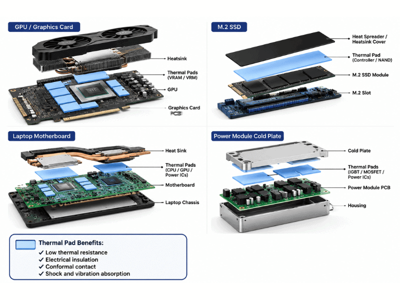
Application selection matrix
| Application | Geometry to map | Main mechanical risk | Other critical checks |
|---|---|---|---|
| GPU VRAM | Package-to-cooler gap at every chip | Cooler lift and die-contact loss | Conductivity, softness, rework |
| GPU/board VRM | Mixed MOSFET, choke, and driver heights | Uneven force and missed devices | Electrical insulation, hotspot load |
| M.2 SSD | Controller/NAND-to-spreader gap | Bending a thin module | One- or two-sided cooling, adhesive |
| Laptop | Tight z-height and multiple heat paths | Chassis distortion | Battery proximity, serviceability |
| Power electronics | Module/case-to-cold-plate gap | Package and solder-joint load | Isolation, cycling, vibration, flame rating |
| Automotive control unit | Wide production tolerance population | Long-term compression set | Contamination, reliability, traceability |
Start with the complete thickness selection workflow, then apply the checks below.
Use power and area as inputs—not universal cutoffs
Application names help locate the pad, but they do not define its thermal duty. Two devices with the same total power can present very different interface conditions when their active heat-source area, package spreading, and cooler contact area differ. Use heat flux = heat flow / active area as a screening calculation, then confirm the real temperature distribution because the package footprint is not always the active heat-source footprint.
Area also changes the mechanical problem. A wider pad can cross more surface waviness and produce greater total force at the same pressure. For that reason, do not select a material from a fixed power or package-area threshold. Record total heat, estimated heat-flux distribution, contact footprint, gap map, and load limit together; use testing to determine whether the selected pad maintains contact without disturbing adjacent interfaces.
GPU and VRAM thermal pad thickness
On a graphics card, thermal pads commonly connect VRAM and power-stage components to the main cooler or backplate. The GPU die usually uses paste or a phase-change material because its working interface is much thinner.
The central risk is cooler balance. An oversized VRAM pad can hold the cooler away from the die. An undersized pad can leave one or more memory packages with weak contact.
For a repair:
- Confirm the exact card model, PCB revision, and cooler revision.
- Photograph every original pad location.
- Check service data before relying on community lists.
- Map each gap or measure the least-deformed original regions with low force.
- Verify the GPU die interface after reassembly.
- Compare temperatures under the same power, fan curve, and ambient conditions.
Do not assume all VRAM positions use one thickness. Cooler machining and package heights can create zones.
VRM and MOSFET arrays
VRM regions combine small packages, different heights, exposed conductors, and uneven heat generation. A soft pad can share load across the array, but too much thickness can push hard on the tallest package while barely improving contact on shorter parts.
Check:
- Minimum and maximum device height
- Cold-plate flatness
- Pad contact area beyond the package body
- Breakdown voltage and volume resistivity
- Local pressure on delicate packages
- Thermal cycling and vibration
If height variation exceeds the comfortable range of one sheet grade, use zoned thicknesses or evaluate a dispensable gap filler.
M.2 SSD thermal pad thickness
M.2 modules are thin and easy to bend. The controller, NAND packages, and other components may not share one height.
Before selecting a pad:
- Determine whether the heat spreader contacts the top, bottom, or both sides.
- Check whether the enclosure closes on hard stops.
- Map the controller and memory heights separately.
- Include adhesive-liner thickness if the product uses tack.
- Make sure pressure does not bow the module or connector.
Use the thinnest validated pad that maintains full contact. A thick “universal SSD pad” can transfer enclosure load into the module instead of merely transferring heat.
Laptops and compact consumer electronics
Compact devices route heat through covers, frames, shields, heat pipes, and multiple TIM types. Space is limited, so changing one pad can disturb another interface.
Jiuju’s consumer electronics thermal solutions cover smartphones, laptops, consoles, smart-home devices, and wearables. For any of these, the controlling inputs are the actual z-height, touch-temperature target, board stiffness, and rework process—not a generic device name.
Contamination-sensitive cameras or sensors may also require low-bleed or non-silicone materials. That constraint should be set before narrowing the thickness.
Power electronics and industrial modules
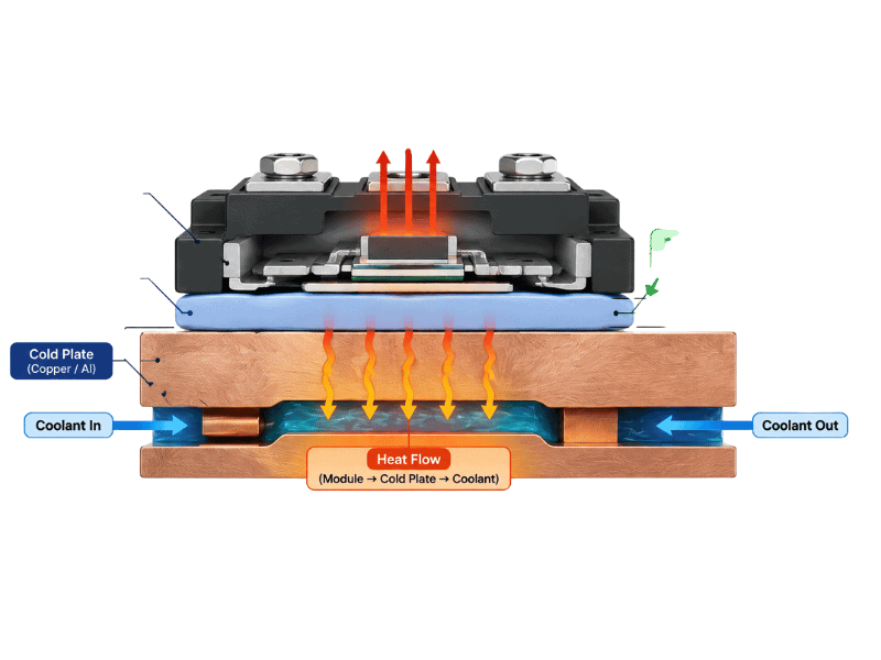
Power converters, IGBT/MOSFET assemblies, industrial controllers, and battery systems often have larger contact areas and wider tolerance stacks than consumer devices. A pad can provide thermal transfer, electrical isolation, and tolerance absorption, but it also applies a distributed load.
Release criteria should include:
- Power loss and allowed temperature rise
- Contact area and heat-flux distribution
- Minimum and maximum gap across production units
- Module, PCB, and cold-plate load limits
- Compression-deflection curve
- Dielectric requirements after compression
- Temperature cycling, vibration, and aging
- Inspection method and lot traceability
ASTM D5470 provides a standard framework for thermal impedance measurement, while ASTM D575 characterizes compression-deflection behavior. Neither replaces testing in the final assembly.
Should you use an application thickness chart?
Use it only as a purchasing or prototype checklist. Common nominal sizes—0.5, 1.0, 1.5, and 2.0 mm—help you plan samples. They do not establish compatibility.
The correct sequence is:
- Specification from the exact hardware maker
- Measured gap map
- Calculated thickness and worst-case compression
- Force and seating validation
- Controlled thermal and reliability test
Compare common sizes in 0.5mm vs 1mm vs 1.5mm vs 2mm Thermal Pads.
Manufacturing experience to include in the specification
Jiuju reports thermal-pad availability from 0.3 mm to 15 mm by customization, typical standard thickness tolerance of ±10%, and optional ±5% control. It also reports that shipment inspection can include conductivity, Shore 00 hardness, dimensions, appearance, and agreed customer tests.
Use those as discussion points. The purchase drawing should still state:
- Grade and revision
- Thickness and tolerance
- Die-cut geometry and location
- Adhesive or no adhesive
- Test method and acceptance limits
- Inspection frequency
- Packaging, liner, and traceability
Match validation to the application failure mode
The same nominal pad can face very different risks in a graphics card, optical module, vehicle controller, or power converter. A useful qualification plan starts with the application failure, then chooses tests—not the other way around.
| Application risk | Evidence to collect before release |
|---|---|
| Cooler lift over a GPU or CPU die | Hard-stop seating, torque, contact print, die-interface result and board flatness |
| Mixed-height VRAM or VRM array | Multi-point gap map, compression-force curve and witness marks on every device |
| Thin M.2 module | Module bow, controller/NAND contact, enclosure closure and repeated assembly |
| Large power interface | Total force, dielectric performance at compressed thickness, thermal impedance and cycling |
| Optical or sensing enclosure | Volatile content, oil bleed, material compatibility and visual contamination inspection |
| Automotive or industrial controller | Thermal cycling, damp heat, vibration as required, traceability and post-test thermal/mechanical checks |
Jiuju’s documented development workflow includes APQP and DFMEA/PFMEA. Used correctly, these tools link a risk such as “pad lifts the cooler” to the design control, process control, measurement method and reaction plan. They should result in concrete drawing fields and inspection records, not extra acronyms in the qualification report.
The available internal test menu includes high- and low-temperature exposure, damp heat, thermal cycling or shock, volatility and oil-bleed evaluation. Conditions and pass limits should be grade- and project-specific. For a shipment report, Jiuju states that conductivity, Shore 00 hardness, dimensions, appearance and agreed customer tests can be included. Define which are per lot, periodic, qualification-only or third-party checks.
When a field issue occurs, preserve the lot, assembly history, contact print, deformation and contamination evidence. Jiuju documents an issue-evaluation-to-8D loop; the quality of that loop depends on receiving a reproducible failure, not only a photograph of a hot component.
FAQ
What thickness thermal pad should I use for GPU VRAM?
Use the value for the exact card and cooler revision. If it is unavailable, measure every VRAM gap and verify that the selected pad does not lift the cooler from the GPU die.
What thickness thermal pad should I use for an M.2 SSD?
The size that bridges the controller/NAND-to-spreader gap without bending the module. Enclosures and heatsinks vary, so measure the assembly.
Do power electronics need thicker thermal pads?
They may have wider gaps, but thickness is determined by mechanical geometry and force limits. Large area can make even modest pressure create substantial total force.
Treat every application as an assembly
GPU, SSD, VRAM, VRM, and power-electronics labels describe where the pad works—not how thick it should be. Measure the assembly, include tolerance extremes, and validate contact and force.
Use Jiuju’s thermal pad products to shortlist material families, then release a grade and thickness only after the mechanical and thermal checks pass.