A thermal pad is probably too thin when it fails to touch both surfaces. It is probably too thick when it prevents the assembly from seating or creates excessive compression force. Temperature alone cannot tell you which failure you have; both conditions can make a component run hot.
Use contact prints, mechanical seating, board flatness, and controlled thermal tests together. This guide shows you what to look for and what to change.
Fast diagnosis table
| Symptom | More consistent with too thin | More consistent with too thick |
|---|---|---|
| No contact mark on one pad face | Yes | Sometimes, if the cooler tilts |
| Heatsink or lid will not seat | No | Yes |
| PCB bows near the interface | No | Yes |
| Temperature changes when pressing the lid | Yes | Yes |
| Adjacent paste interface loses contact | No | Yes |
| Pad shows almost no compression | Yes | Possible with a hard oversized pad |
| Pad extrudes or wrinkles | No | Yes |
| Only the tallest component has a clear print | Yes | Possible in a multi-height array |
The symptoms overlap because pad thickness affects the whole mechanical stack. Start with geometry, not assumptions.

Signs a thermal pad is too thin
Missing or one-sided contact print
A properly fitted pad normally shows evidence of contact on both mating faces. If one side is pristine, the pad may never have bridged the gap. Check several locations because a tilted cooler can contact one edge and miss another.
Hotspot remains after pad replacement
If the material rating improved but the hotspot did not, the new pad may be thinner, harder, or less conformable than the original. A high conductivity number does not compensate for an air gap.
Performance changes when you press the enclosure
If light external pressure temporarily lowers temperature, contact is pressure-sensitive. The pad may be too thin, the mounting load may be insufficient, or the structure may be flexing.
Uneven component array contact
On VRMs, memory packages, or power stages, the tallest devices may print clearly while shorter devices remain untouched. The fix may require a softer or thicker pad, tighter component-height control, a compliant cold plate, or different pad zones.
Risks of a pad that is too thin
- Air gaps and sharply higher interface resistance
- Localized hotspots
- Unit-to-unit thermal variation
- Intermittent contact under vibration or thermal cycling
- Misleading pass results on a single favorable sample
The remedy is not automatically the next catalog thickness. Measure the minimum and maximum gap first using the method in How to Measure Thermal Pad Thickness and Component Gap.
Signs a thermal pad is too thick
The assembly does not reach its hard stops
Inspect screw bosses, lid edges, and designed seating surfaces. If a visible gap remains after the correct torque sequence, the pad may be holding the joint open.
PCB bow or package tilt
Use a straightedge, displacement measurement, or CMM comparison before and after installation. Local bow near a BGA or ceramic package deserves immediate attention.
A neighboring thermal interface gets worse
An oversized pad on VRAM can lift a GPU cooler away from the die. The VRAM may cool while the GPU core heats up—or both may get worse because the cooler tilts.
Extrusion, edge roll, or tearing
Visible deformation can indicate excess strain, poor lateral constraint, or an unsuitable reinforcement. It can also signal a cutting or placement issue, so verify the geometry before blaming thickness alone.
Risks of a pad that is too thick
- Longer conduction path and higher bulk resistance
- Excess load on components, solder joints, and PCB
- Incomplete screw engagement or uneven torque
- Cooler tilt and loss of contact at adjacent interfaces
- Pad creep, extrusion, or shift
- Assembly-height and enclosure-fit problems
Sizing Decision Matrix: Too Thin vs. Too Thick
Before tearing down the hardware or altering pad dimensions, evaluate the failure mode against this quick-reference summary:
| Evaluation Metric | When the Pad Is Too Thin | When the Pad Is Too Thick | Target Engineering Balance |
| Primary Failure Mechanism | Interfacial air gaps and micro-voids | PCB bending and mechanical standoff lift | Full surface wetting under permissible load |
| Thermal Symptom | Localized hotspot; sensitive to hand pressure | Elevated baseline temperature or core die overheat | Stable, low thermal impedance ($R_{\text{total}}$) |
| Mechanical Symptom | Zero compression marks; uncompressed pad face | Bowed circuit board; screw standoffs unseated | 15% to 30% controlled strain across tolerance stack |
| Adjacent Interfaces | Unaffected by pad load | Neighboring thermal paste/PCM delaminates | Uniform, coplanar cooler seating |
| Primary Engineering Risk | Thermal runaway and solder fatigue | Crushed silicon dies and sheared solder balls | Long-term reliability without physical strain |
| Immediate Corrective Action | Increase nominal thickness or choose a softer grade | Decrease nominal thickness or lower Shore 00 hardness | Validate against ASTM D575 deflection curves |
Decision Rule: Which Way to Adjust?
Redesign the Joint: If the gap variation across an array exceeds the usable deflection range of a single pad sheet, switch to multi-zone thickness pads, a stepped cold plate, or a dispensable thermal putty/gel.
Shift Thicker (or Softer): Only if you observe untouched pad faces, localized overheating on low-profile components, or temperature drops when manually pressing the heatsink.
Shift Thinner (or Softer): Whenever heatsink standoffs fail to bottom out, the board visibly bows, or an adjacent processor core suddenly overheats after tightening the cooler.
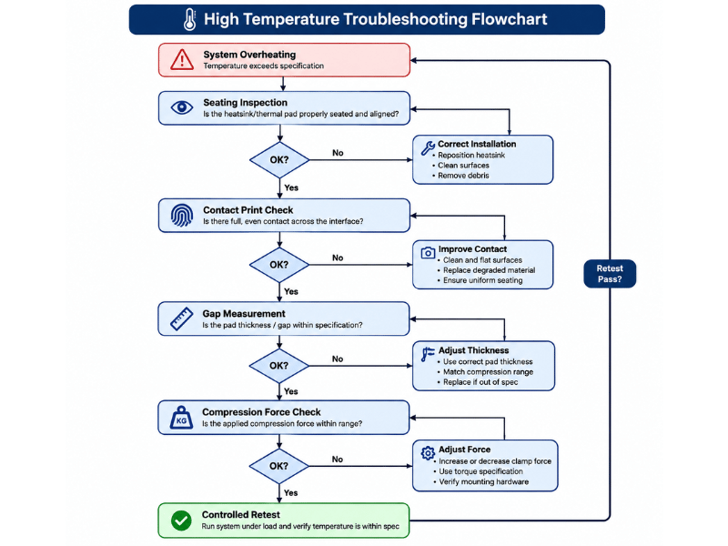
A five-step troubleshooting process
1. Reproduce the problem
Control power, ambient temperature, airflow, fan curve, sensor location, software load, and warm-up time. A before/after temperature comparison is useless if the fan profile changed.
2. Inspect mechanical seating
Confirm fasteners, washers, spacers, gasket, torque, tightening sequence, and hard-stop closure. Never solve a missing spacer with more thermal pad.
3. Read the contact print
Photograph both pad faces. Look for full-area print, edge-only print, torn regions, wrinkles, contamination, and differences across the component array.
4. Measure the gap and calculate compression
Use:
Compression = (free pad thickness − installed gap) / free pad thickness
Then include pad and assembly tolerances. The pillar selection guide provides the worst-case formulas.
5. Compare force and thermal results
Check the exact grade’s compression-deflection curve. ASTM D575 is designed to compare rubber stiffness in compression. For thermal results, ASTM D5470 explains why impedance depends on interface conditions as well as material thickness.
Solutions by root cause
| Root cause | Corrective action |
|---|---|
| Pad does not bridge maximum gap | Increase thickness or use a more conformable grade after force check |
| Pad overloads minimum gap | Reduce thickness, select a softer grade, or redesign the stop/load path |
| Wide multi-height variation | Use zoned thicknesses, a stepped spreader, or dispensable gap filler |
| Pad tolerance creates unstable compression | Specify tighter thickness control and incoming measurement method |
| Cooler tilts | Balance pad zones and verify fastener sequence and hard stops |
| Assembly force is unknown | Obtain pressure-deflection data and define component load limits |
| Irregular gap defeats sheet pad | Compare thermal pad vs thermal putty |
When thickness is not the root cause
A joint can pass the initial contact check and still fail later. Do not keep changing pad thickness if the evidence points to material movement, contamination, or environmental aging.
Inspect the complete cooler stack before blaming the pad. Many assemblies use a pad over memory or power devices and paste or a phase-change material over a nearby die. An over-compressed pad can lift or tilt the cooler and weaken that neighboring interface; conversely, pump-out or dry-out at the thin interface can raise temperature even when the pad thickness is correct. Check seating, contact prints, and interface condition at every thermal zone that shares the same load path.
Total power alone does not identify the failed interface. Compare hotspot location and effective contact area: a concentrated hotspot points to a different problem from a broad temperature rise across the whole cooler. Use that pattern to decide which interface to open and measure first.
Jiuju’s internal reliability menu includes high-temperature and low-temperature exposure, damp heat, thermal cycling or shock, volatility, and oil-bleed evaluations. The exact condition and acceptance limit must be defined for the selected grade and project; a generic chamber test is not a universal pass. Compare appearance, thermal resistance or conductivity, hardness, displacement, electrical behavior, and contamination before and after the relevant exposure.
Oil bleed is especially easy to misdiagnose as a thickness problem. Mobile species can create haze near optics, soil a PCB or contact, contribute to leakage paths, and leave the remaining pad less stable at the interface. A hotter result after aging may therefore come from changed contact or material composition, not from an incorrect original nominal thickness.
Use the failure pattern to separate causes:
- Failure is immediate and repeatable with assembly: Recheck gap, pad thickness, hard stops, torque and force.
- Failure grows with time at temperature: Check bleed, volatile loss, relaxation, pump-out and adjacent materials.
- Failure appears after cycling or vibration: Check layer shift, edge extrusion, fastener relaxation and intermittent contact.
- Failure varies by lot: Compare incoming dimensions, hardness, formulation-control records and shipment data.
- Failure is limited to optics or high-impedance circuits: Add contamination and electrical-resistance investigation before changing thickness.
Photograph the as-found condition before cleaning or disassembly. Record time, temperature history and lot number. That evidence gives a supplier’s issue-evaluation or 8D process something concrete to test.
FAQ
Will a thicker thermal pad lower temperature?
Only if the current pad is too thin to maintain contact. Once contact is complete, extra thickness usually adds bulk resistance and compression force.
Can a thick thermal pad damage a GPU or PCB?
Yes. Excess force can bow the board, tilt the cooler, stress packages, or disturb the die interface. The risk depends on area, stiffness, mounting design, and material curve.
Should I judge the fit by temperature only?
No. A thermal pass does not prove mechanical reliability, and a high temperature does not identify the thickness error. Combine thermal, contact, and deformation evidence.
Fix the stack, not just the pad
When a thermal pad is too thick or too thin, the visible pad is only one part of the problem. The real design is the full stack: gap, tolerances, force path, material, cooler, and adjacent interfaces.
For a production correction, document the gap range and failure evidence, then compare it with Jiuju’s thermal pad specifications. Request a grade-level force curve and define the critical shipment checks before changing the drawing.