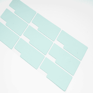
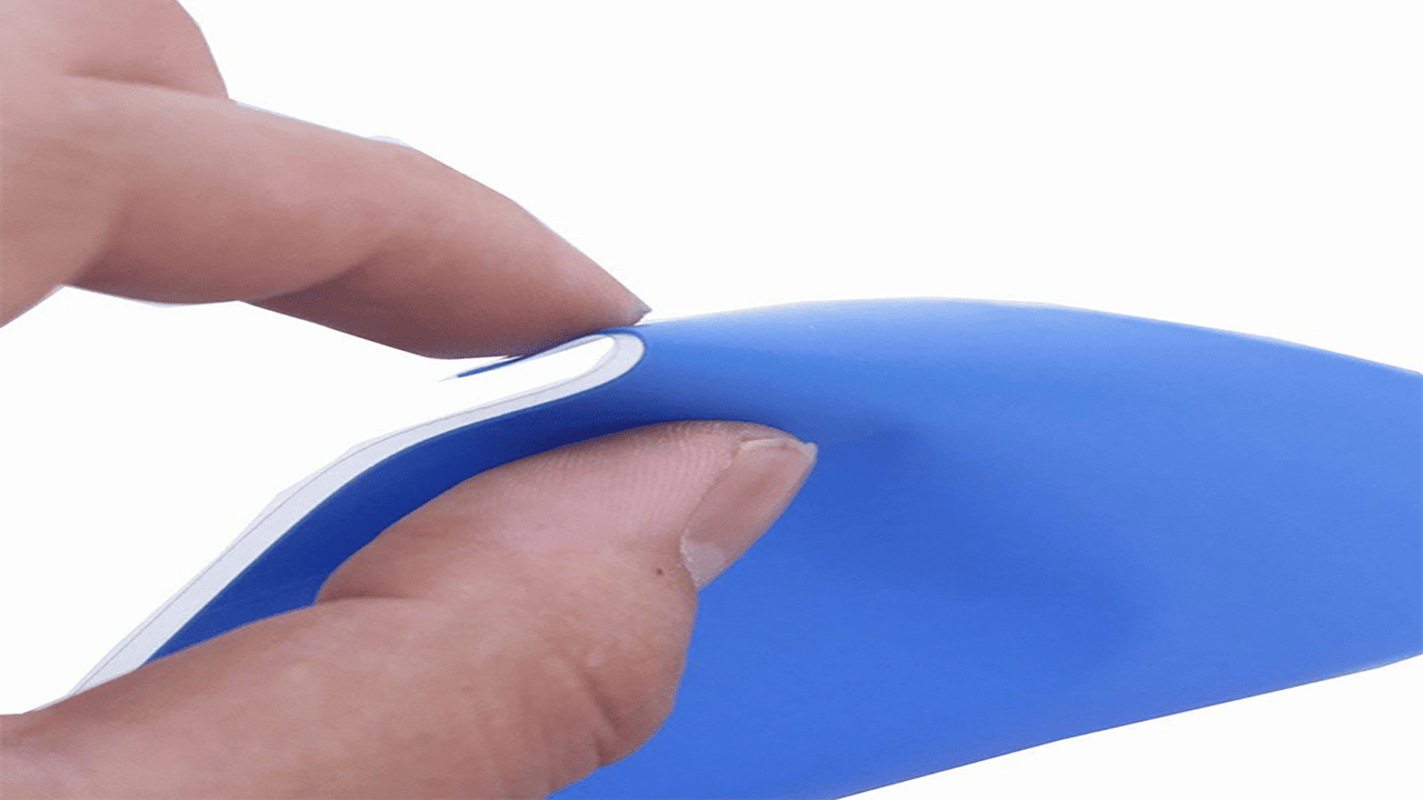
A nominal 1.0 mm gap on CAD is rarely 1.0 mm on the production line.
Tolerance stackup—driven by component height variance, PCB warpage, pad manufacturing tolerances, and fastener preload—makes generic sizing charts a major reliability risk. Sizing by guesswork leads to two distinct failure modes:
- Over-thickness: Excessive clamp stress causes board flex, solder joint cracking, and heatsink tilt.
- Under-thickness: Incomplete surface wetting leaves microscopic air voids, leading to localized hotspots and thermal runaway.
The Golden Rule: The optimal thermal pad is the thinnest grade that guarantees complete contact across worst-case mechanical tolerances without exceeding the mechanical load limit of the components.
This guide provides a repeatable, thermal-mechanical selection framework to measure actual assembly gaps, calculate nominal thickness with tolerance extremes, and validate thermal impedance alongside mechanical stress.
Sizing Principle
Use this sequence:
- Measure the assembled gap at every thermal contact point.
- Find the minimum and maximum gap across location, tolerance, and units.
- Choose a material and obtain its compression-force data.
- Calculate a nominal pad thickness that keeps every unit inside the approved compression window.
- Verify contact, board deflection, fastener seating, and temperature in the real assembly.
Do not select thickness from thermal conductivity alone. A 10 W/m·K pad that barely touches one surface can perform worse than a lower-conductivity pad with complete, controlled contact.
Thermal-Mechanical Trade-offs
A thermal pad has two jobs. It must replace insulating air in the gap, and it must create a practical heat path without applying destructive force.
For a simple one-dimensional comparison, bulk thermal resistance increases with thickness:
Rbulk ≈ t / (k × A)
where t is bond-line thickness, k is apparent thermal conductivity, and A is contact area. Real interfaces also include contact resistance at both surfaces. Pressure, flatness, roughness, and pad conformity change those terms.
That is why a datasheet conductivity value is not a system result. ASTM D5470 measures steady-state thermal impedance under controlled conditions and explicitly notes that its idealized heat flow does not directly reproduce most applications. It also explains that testing multiple specimen thicknesses can separate bulk and contact resistance.
Thickness creates a two-sided risk:
- Too thin: incomplete contact, air gaps, localized hotspots, and unstable performance.
- Too thick: a longer heat path, excessive compression force, heatsink tilt, incomplete fastener seating, or PCB/component stress.
The best selection is not “as thick as possible” or even “as thin as possible.” It is as thin as the assembly can reliably tolerate while maintaining full contact.
Key Gap Dimensions
Before calculating anything, keep these values separate.
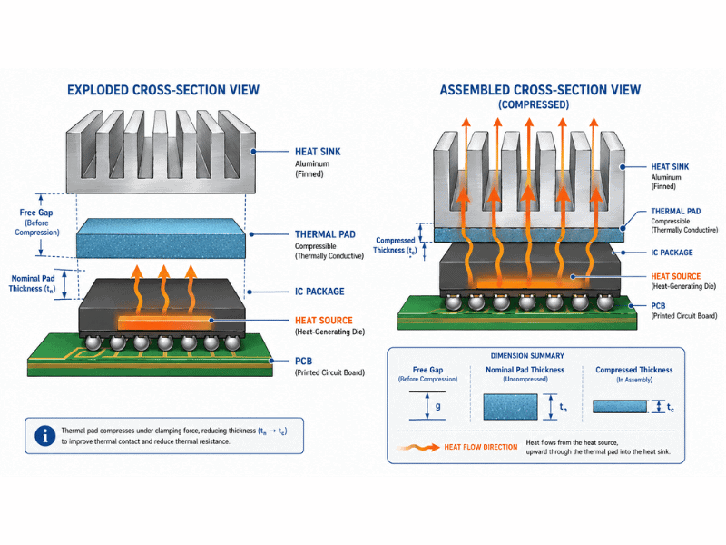
Free gap
The distance between the heat source and the cooling surface before the thermal pad is installed, with the assembly held in its intended mechanical position.
Nominal pad thickness
The thickness printed on the drawing, label, or datasheet before installation.
Actual pad thickness
The manufactured thickness of a specific pad. It differs from nominal by the product tolerance.
Compressed thickness
The pad thickness after the enclosure or heatsink is fastened. In a well-seated assembly, this should be close to the working gap at that location.
Compression ratio is:
Compression = (free pad thickness − compressed thickness) / free pad thickness
Always state it as a percentage and pair it with pressure or force. “20% compression” without the force needed to reach it is only half a specification.
4-Step Selection Process
Step 1: Measure the real assembly gap
Measure the gap in the state that represents production: the correct fasteners, torque sequence, gasket, enclosure, board supports, and mating parts. A loose mock-up can misrepresent the final geometry.
Use more than one point. A cold plate may be flat while the PCB bends. One corner can show a 0.8 mm gap and another 1.1 mm. Your pad must handle the range without turning the board into a spring experiment.
Practical methods include:
- Coordinate measuring equipment or a height gauge for accessible datum-based assemblies
- Feeler gauges where the geometry permits direct access
- A non-hardening witness material for prototype gap mapping
- Controlled test coupons cut from candidate pad thicknesses
- Cross-section or displacement measurement for high-value validation
Do not clamp a soft used pad with a caliper and treat that reading as the original gap. You may measure your hand pressure more than the part.
For detailed methods, see How to Measure Thermal Pad Thickness and Component Gap Accurately.
Step 2: Define the compression window
Use the supplier’s compression-deflection curve for the exact grade and thickness. ASTM D575 covers compression-deflection testing of rubber compounds and is useful for comparing stiffness in compression.
Your acceptable window depends on:
- Contact needed to wet both surfaces
- Maximum pressure the component, solder joints, and PCB can tolerate
- Fastener load and enclosure stiffness
- Long-term compression set and thermal cycling
- Whether the pad is reinforced or unsupported
- Handling and rework requirements
Avoid a universal compression percentage. Two pads with the same Shore 00 hardness can still produce different force at the same strain because formulation, thickness, reinforcement, and test conditions differ.
Step 3: Calculate a starting nominal thickness
If G is the working gap and C is the target compression ratio, a first estimate is:
Pad thickness T = G / (1 − C)
For a measured 1.20 mm gap and a supplier-approved target of 20%:
T = 1.20 / (1 − 0.20) = 1.50 mm
That makes 1.5 mm a sensible prototype—not an automatic production release.
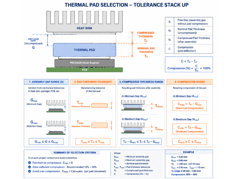
Step 4: Check the tolerance extremes
Now test the worst cases.
Minimum compression = 1 − (maximum gap / minimum pad thickness)
Maximum compression = 1 − (minimum gap / maximum pad thickness)
Suppose the assembly gap is 1.20 ± 0.10 mm and the 1.50 mm pad has a ±10% thickness tolerance:
- Maximum gap: 1.30 mm
- Minimum gap: 1.10 mm
- Minimum pad thickness: 1.35 mm
- Maximum pad thickness: 1.65 mm
- Minimum compression: about 3.7%
- Maximum compression: about 33.3%
The nominal design says 20%. Production can see roughly 4% to 33%. If the material is not validated across that window, change the tolerance, the pad grade, the mounting design, or the nominal thickness.
In Jiuju’s current manufacturing practice, standard thermal-pad thickness tolerance is typically specified at ±10%, with ±5% control available for tighter requirements. Custom thicknesses from 0.3 mm to 15 mm are reported as manufacturable, but the usable range still depends on the exact formulation and drawing. Treat these values as sourcing inputs, then confirm them on the released specification.
Nominal Thickness Matrix
Replacement projects need extra care because the removed pad has already been compressed, heated, and aged.
- Photograph and label every pad location before removal.
- Record orientation, part number, and whether the pad has carrier or adhesive films.
- Measure several undamaged areas with a low-force thickness gauge if available.
- Compare witness marks on both sides. A one-sided print suggests incomplete contact.
- Check the service manual or original drawing before choosing a replacement.
- Reassemble and validate temperatures at the same load, fan control, and ambient conditions.
A caliper can help with firmer pads, but its jaw force can compress soft grades. For production inspection, define the gauge force and method instead of writing only “measure thickness.”
Key Material Properties
Standard sizes such as 0.5, 1.0, 1.5, and 2.0 mm are convenient inventory choices. They are not universal component rules.
| Nominal thickness | Useful starting situation | Main risk to check |
|---|---|---|
| 0.5 mm | Tight, well-controlled gaps and flat interfaces | Missed contact at tall tolerance locations |
| 1.0 mm | Moderate gap with limited height variation | Force rise if the real gap is smaller than expected |
| 1.5 mm | Larger variation or uneven component heights | Added bulk resistance and heatsink tilt |
| 2.0 mm | Wide gaps and compliant enclosure designs | Excess force, long heat path, and lateral shift |
The final choice comes from the measured gap and the pad’s force-deflection curve. The component name alone is not enough. The same GPU family can use different gaps across board partners and cooler revisions.
For a focused comparison, read 0.5mm vs 1mm vs 1.5mm vs 2mm Thermal Pads.
Diagnostic Symptoms
Thermal conductivity and impedance
Higher conductivity can reduce bulk resistance, but thickness and contact dominate when the pad is poorly fitted. Compare thermal impedance at a relevant thickness and pressure whenever suppliers provide it, not conductivity in isolation.
Jiuju reports a 1.2–25 W/m·K thermal-pad range, with JIUJU625X identified as the top reported grade. Standard published models currently cover lower conductivity values on the thermal pad specification page. Request the current TDS and test conditions before designing around any value.
Hardness and compression force
Softness helps a pad conform at lower load. Hardness, however, is not a direct substitute for compression-force data. Confirm the scale: Jiuju thermal pads use Shore 00, not Shore A. Jiuju reports high-conductivity grades in the 8–25 W/m·K group at 40–60 Shore 00, subject to grade-level confirmation.
Read How Thermal Pad Hardness Affects Thickness Selection before substituting one formulation for another.
Electrical insulation
If a pad crosses exposed conductors, check breakdown voltage, dielectric strength, volume resistivity, and minimum thickness after compression. Do not assume every thermally conductive sheet is electrically insulating.
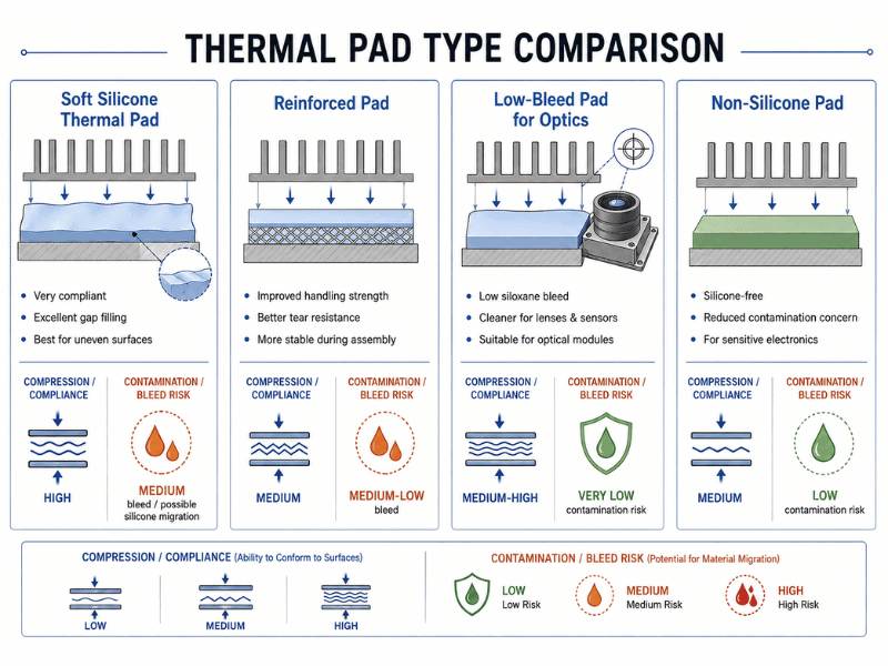
Silicone, low-bleed, and non-silicone options
Optics, sensors, relays, and contamination-sensitive enclosures may need low-bleed or non-silicone materials. Jiuju reports:
- JIUJU-F6000 non-silicone pads from 1.2 to 8.0 W/m·K
- Specific F6300–F6800 grades from 3.0 to 8.0 W/m·K
- A reported volatile mass-loss limit of ≤0.5% after 120°C for 72 hours for the non-silicone series
- Low-bleed grades from JIUJU6600LB through JIUJU625XLB, with an internal 125°C/14-day oil-ring test reported below 3 mm
These are manufacturer-reported capabilities, not universal industry limits. Ask for the exact report, specimen thickness, conditioning, acceptance method, and lot applicability.
Measuring Existing Pads
Signs the pad may be too thin
- No witness mark on one side
- Hotspot remains despite a reasonable material rating
- Performance changes when the enclosure is pressed by hand
- Some components contact while shorter neighbors do not
- Thermal image shows a localized break in the heat path
Signs the pad may be too thick
- Heatsink or lid does not seat against its stops
- Screw torque rises before the joint closes
- PCB bows or components tilt
- Adjacent paste interface loses contact
- Temperature increases after installing a “better” but thicker pad
- Pad extrudes, wrinkles, or tears at the edges
See Thermal Pad Too Thick or Too Thin? for a diagnostic workflow.
Application Guidelines
Use the hardware manufacturer’s drawing or service data first. If it is unavailable, measure the exact unit and treat common sizes only as prototype inventory.
- GPU VRAM and VRM: Map every device height. Confirm that the pad does not lift the cooler away from the GPU die or paste interface.
- M.2 SSD: Check whether the heat spreader contacts one side or both, and whether NAND packages and controller heights differ.
- Power modules and converters: Include isolation, fastener load, vibration, flatness, and temperature cycling in the release criteria.
- Battery packs and automotive electronics: Design for a population of gaps, not one golden sample. Automation and rework can matter as much as conductivity.
- Optical and sensing systems: Add contamination and volatile requirements before screening thickness.
For a deeper application breakdown, see Thermal Pad Thickness by Application and Jiuju’s consumer electronics thermal solutions.
Production validation checklist
Before releasing the pad drawing, verify:
Jiuju reports that shipment reports for thermal pads can include conductivity, hardness, dimensions, appearance, and customer-defined test items. Non-core and reliability testing may follow different frequencies unless the project specifically requires per-lot control. Put the required frequency and acceptance limits on the purchase specification; do not rely on a verbal “tested” label.
Build a data package that follows the risk
A reliable supplier validation package extends far beyond a nominal thermal conductivity value on a catalog sheet. For thickness- and stress-critical interfaces, the supplier’s test criteria must correlate directly with mechanical drawing tolerances and application-specific risk profiles:
- Optical & Camera Modules: Focus on tight thickness tolerances, low volatile condensable material (CVCM), zero siloxane outgassing, and oil-bleed limits to prevent lens contamination.
- Power Electronics & Converters: Require compression-force deflection (ASTM D575) data, dielectric breakdown voltage, volume resistivity, and thermal impedance under thermal shock.
- Automotive & Battery Packs (BESS): Emphasize large-area coplanarity, continuous clamping force retention, vibration resistance, and long-term compression set.
Quality framework artifacts—such as APQP deliverables, DFMEA/PFMEA, and 8D root-cause tracking—serve as the foundation for traceability. They ensure nominal dimensions, lot-to-lot tolerances, measurement methods (e.g., low-force gauge thickness, ASTM D5470 thermal testing), and sampling frequencies remain tightly linked throughout volume manufacturing.
Pre-Approval Verification Checklist
Before signing off on the thermal interface drawing, request and verify the following from your supplier:
- Grade-specific Technical Data Sheet (TDS) and ASTM D575 stress-strain curve.
- Lot-specific Certificate of Analysis (COA) / shipment report reflecting actual dimensional and Shore 00 hardness test methods.
- Outgassing, oil-bleed, or electrical isolation test reports matching your exact assembly pressure and operating temperature envelope.
Production Validation
Share your working gap dimensions (Gmin/Gmax), target clamping pressure, thermal conductivity targets, and isolation requirements with our engineering team.

FAQ
Should a thermal pad be thicker than the measured gap?
Usually, yes, because a compressible pad needs some interference to maintain contact. The required amount comes from the grade’s validated compression range and force curve, not a universal percentage.
Is a thinner thermal pad always better?
Only when it still fills the complete worst-case gap. A thinner heat path helps bulk resistance, but an air gap can erase that advantage.
Can I stack thermal pads to reach the required thickness?
Stacking can work as a prototype or repair contingency, but an extra internal interface adds uncertainty and the layers can shift. A single specified thickness is usually easier to control in production. See Can You Stack Thermal Pads?.
How much should a thermal pad compress?
Enough to create full contact, but not enough to exceed the assembly’s force budget or the supplier’s validated strain. Use compression-deflection data for the exact pad. See How Much Should a Thermal Pad Compress?.
When is thermal putty better than a pad?
Putty or dispensable gap filler can suit wide, irregular, or multi-height gaps where a sheet pad would need excessive thickness or many part numbers. Process control, pump-out, rework, and dispensing volume then become important. Compare them in Thermal Pad vs Thermal Putty for Uneven Gaps.
Choose the thickness from the assembly, not the shelf
The best thermal pad thickness is a controlled mechanical fit that also meets the thermal target. Measure the real gap, calculate the tolerance extremes, check the force curve, and validate the assembled hardware. That process takes longer than copying a size from a forum, but much less time than debugging a warped board.
If you are selecting a grade for production, send Jiuju the minimum and maximum gap, contact area, mounting method, pressure limit, operating temperature, insulation needs, and contamination requirements. The team can recommend a thermal pad option and align the shipment report with your critical checks.