Why does a device often run hotter after upgrading to a thicker, higher-rated thermal pad?
Choosing between 0.5 mm, 1 mm, 1.5 mm, and 2 mm pads is a strict balance of bulk thermal resistance against mechanical clamping stress. The following guide breaks down the performance trade-offs of each standard thickness, maps their mechanical limits, and shows how to calculate the exact compressed fit for your hardware.
Quick comparison
| Pad thickness | Best starting point | Advantage | Main risk |
|---|---|---|---|
| 0.5 mm | Tight, flat, well-controlled interfaces | Short heat path | Missed contact if the gap varies |
| 1.0 mm | Moderate gaps with reasonable planarity | Common balance of fit and resistance | Can overload a gap well below 1 mm |
| 1.5 mm | Larger gaps or mixed component heights | More conformity range | Higher bulk resistance and force variation |
| 2.0 mm | Wide gaps and compliant structures | Bridges substantial separation | Heatsink lift, board bow, and lateral movement |
These are starting conditions, not a device compatibility chart. Read the complete thermal pad thickness selection guide before releasing a drawing.
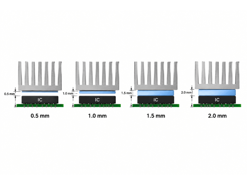
0.5 mm thermal pads
A 0.5 mm pad suits a narrow gap with tight flatness and height control. Because the conduction path is short, it can offer lower bulk resistance than a thicker pad made from the same material.
Its weakness is tolerance. If one corner opens beyond the pad’s usable compressed range, contact disappears quickly. Check lid flatness, PCB bow, component coplanarity, adhesive thickness, and pad tolerance.
Use 0.5 mm only when your measurements show enough interference for contact at the largest gap and acceptable force at the smallest gap.
1 mm thermal pads
One millimeter is popular because it can absorb more height variation while remaining manageable in cutting and assembly. It is often a useful prototype size for moderate gaps.
Do not force a 1 mm pad into a much smaller space. The percentage compression may look tolerable, yet the required force can still exceed the PCB or package limit. Obtain the exact grade’s compression-deflection curve.
1.5 mm thermal pads
A 1.5 mm pad provides more compliance for uneven surfaces, mixed component heights, and enclosures with larger tolerance stacks. It can be a practical fit for VRM arrays, power devices, and housings—but only after measurement.
The added thickness increases bulk resistance for the same conductivity and area. It also magnifies thickness-tolerance effects. At Jiuju’s typical reported ±10% standard thickness tolerance, a nominal 1.5 mm pad could span a wider absolute range than a 0.5 mm pad. Tighter ±5% control is reported as available when specified and confirmed.
2 mm thermal pads
A 2 mm pad is a gap filler, not a universal upgrade. It can bridge a large separation where a thin interface cannot maintain contact.
Check four failure modes carefully:
- The cooler stops on the pad before the fastener joint closes.
- The PCB bows as the pad pushes back.
- A neighboring paste or phase-change interface loses contact.
- The pad shifts sideways during compression or vibration.
If the gap is highly irregular, a dispensable material may be easier to control than a thick sheet. See thermal pad vs thermal putty.
Pad vs. Alternative TIMs
Compare 0.5 mm, 1 mm, 1.5 mm, and 2 mm only after confirming that the joint needs a compressible sheet. If two surfaces already approach each other closely and the main job is to wet microscopic roughness, paste or a phase-change material may suit the interface better. If the joint has a measurable gap and must absorb a controlled tolerance range, a pad is a logical candidate. Highly irregular or multi-height gaps may favor a dispensable gap filler.
This decision comes before the conductivity number. A thick pad used in a thin surface-wetting joint adds an unnecessary heat path and force. Paste used to bridge a structural gap may leave voids or move during service. Define the job of the interface first; then select the pad thickness.
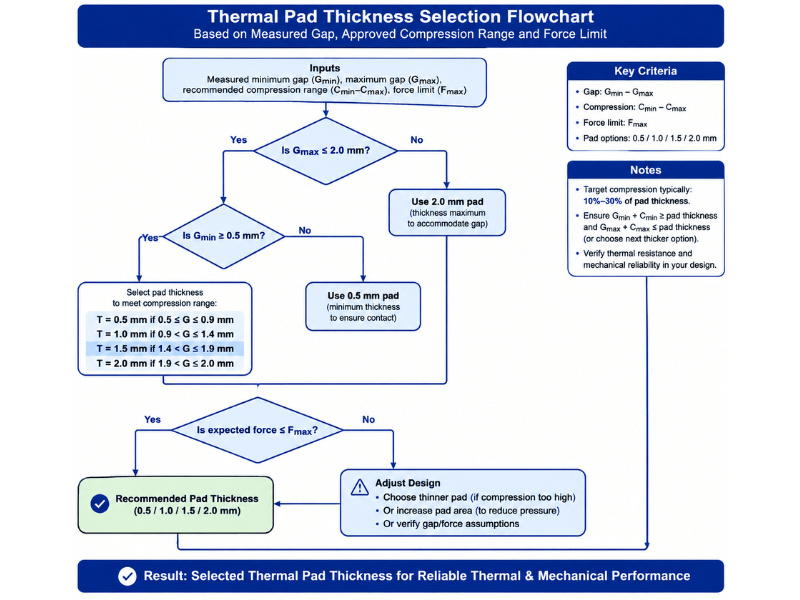
Calculate instead of guessing
For target compression C and measured gap G:
Nominal starting thickness T = G / (1 − C)
If the working gap is 0.80 mm and the chosen grade is validated at a 20% target:
T = 0.80 / 0.80 = 1.00 mm
Then check the minimum and maximum gap, plus pad tolerance. The calculation chooses a prototype. The force curve and assembly test decide whether it survives production.
ASTM D5470 is useful context because it separates thermal impedance from an isolated conductivity number. ASTM D575 covers compression-deflection characterization for rubber compounds.
What matters besides thickness
- Hardness: Confirm the durometer scale. Jiuju pad specifications use Shore 00.
- Compression force: Use the curve for the exact grade and thickness.
- Conductivity and impedance: Compare at relevant pressure and thickness.
- Electrical insulation: Verify the compressed thickness still meets the electrical design.
- Reinforcement: A carrier can improve handling but change conformity.
- Contamination: Low-bleed or non-silicone options may be needed near optics and sensors.
- Tolerance: Include both the part gap and pad thickness variation.
Jiuju publishes standard grade data on its thermal pad specifications page. For values not listed there, request the current TDS and test report rather than relying on a family-range claim.
Nominal vs. Compressed Fit
A label such as “1 mm” identifies a nominal dimension. The delivered part still has a tolerance, and the installed bond line depends on the grade’s compression response. This is why two 1 mm pads can fit very differently.
As a supplier example, Jiuju reports a typical standard thickness tolerance of ±10%, with optional ±5% control when the grade, construction, quantity, and inspection agreement support it. Under a ±10% specification, a nominal 1.0 mm pad can be accepted from 0.90 to 1.10 mm. A nominal 2.0 mm pad can span 1.80 to 2.20 mm. The percentage is the same, but the 2.0 mm part has four times the absolute range of a 0.5 mm part under the same percentage tolerance.
That range must be combined with the hardware gap:
- Use the thinnest allowed pad with the largest gap to check minimum contact.
- Use the thickest allowed pad with the smallest gap to check maximum compression and force.
- Add adhesive, carrier, die-cut and liner requirements to the released construction.
- Define how incoming thickness is measured, including gauge force and sampling locations.
Do not use a caliper reading from one soft sample as the complete incoming inspection plan. Jiuju’s documented equipment includes a thickness gauge and Shore 00 durometer; a project can also request that dimensions, hardness, conductivity and appearance appear on the agreed shipment report. The report confirms only the listed checks, so put critical acceptance limits and frequency in the quality agreement.
For unusual gaps, Jiuju reports custom nominal pad thicknesses from 0.3 to 15 mm. Treat that as a sourcing capability to confirm for the exact material—not a reason to choose a thick pad before measuring the assembly.
FAQ
Can I replace a 1 mm pad with a 1.5 mm pad?
Only if the smaller gap can accept the resulting compression force and the heatsink still seats correctly. A 0.5 mm increase is large in a compact assembly.
Can I use two 0.5 mm pads instead of one 1 mm pad?
It may work for a prototype, but the added interface and layer movement make the stack less repeatable. A single 1 mm pad is usually better for production. Read Can You Stack Thermal Pads?.
Which thickness is best for a GPU or SSD?
The thickness specified for that exact cooler and board revision. If no reliable specification exists, measure the unit. Generic component tables cannot account for board-partner and enclosure differences.
Select a controlled fit
The Final Verdict: Matching Thickness to Your Design Goal
Selecting among 0.5 mm, 1 mm, 1.5 mm, and 2 mm pads comes down to balancing mechanical compliance against thermal impedance:
- 0.5 mm: Choose for precision-machined, flat interfaces where minimizing thermal resistance is paramount and tolerance stackup is negligible.
- 1.0 mm: The versatile baseline for moderate gaps, offering a reliable balance of thermal performance and strain absorption.
- 1.5 mm: The practical choice for multi-component arrays (e.g., VRMs) or cast enclosures with noticeable height variations.
- 2.0 mm: Best reserved for wide structural gaps where compliant gap bridging is required, provided mechanical stops prevent excessive board flex.
Fast Sizing & Selection Workflow
- Map the True Gap: Measure minimum and maximum clearance under full mechanical fastener torque.
- Account for Tolerance Stackup: Add pad manufacturing tolerances (typically ±10% to ±5%) to hardware dimensional extremes.
- Check the Stress-Strain Curve: Verify that the chosen thickness delivers at least 15–20% compression at the widest gap without exceeding component load limits at the narrowest gap.
- Validate Under Operational Load: Test thermal impedance and mechanical seating under actual operating temperatures and thermal cycling.
Need Help Dialing in the Exact Thickness for Your Production Build?
A minor miscalculation in pad thickness can lead to cracked solder joints or poor thermal contact. Share your CAD gap dimensions, component layout, and allowable clamp pressure with our thermal engineering team. We will analyze your tolerance stackup, recommend the optimal pad grade, and provide customized stress-strain data and validation samples tailored to your hardware.