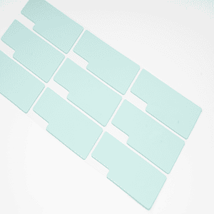

AI clusters are pushing more traffic through the data center front panel. Optical transceivers have to carry that traffic inside compact modules, crowded cages, and tightly controlled airflow. As designs move from 400G to 800G and 1.6T, the available thermal margin can disappear quickly when one interface is too thick, too stiff, poorly seated, or placed in the wrong part of the heat path.
That does not mean every faster module needs the highest-conductivity thermal pad. Data rate is a communication specification, not a complete thermal specification. Two 800G modules can have different DSPs, laser arrangements, power states, housing designs, and host heat sinks. Their thermal interface material requirements may be very different.
Before choosing a material, answer three practical questions:
- Where is the heat generated?
- How does it reach the housing and host cooling system?
- What stops that path from working in the assembled module?
Those answers narrow the material choice more effectively than a conductivity ranking. The remaining decisions involve material form, working thickness, pressure, electrical isolation, cleanliness, and production control. Jiuju’s thermal management solution overview provides a starting point for the available material families.
Why high-speed optical modules are harder to cool
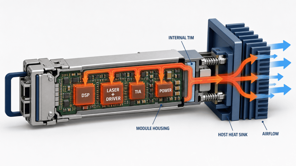
An optical module combines electrical processing, optical conversion, power regulation, and precision mechanical parts in a very small volume. The main heat sources can include the DSP, laser and driver, transimpedance amplifier (TIA), control electronics, and power-conversion components. These parts do not produce the same amount of heat, and they do not share the same temperature limit.
The design team is usually balancing several constraints at once:
- Heat is concentrated over small package areas.
- The module housing has limited space to spread that heat.
- Multiple ports share the same inlet air and front-panel region.
- Surface flatness, component height, and PCB bow create uneven gaps.
- The allowable clamping force may be limited by the package, board, or optical assembly.
- Materials sit close to lenses, connectors, and high-impedance circuits where contamination matters.
- The assembly process has to reproduce the same bond line and contact pressure across production lots.
The cooling path continues beyond the module housing. Heat may leave a component through an internal TIM and the metal shell, but it still has to cross the module-to-host interface, enter the heat sink, and move into the airflow. Similar space, gap, and assembly constraints appear across Jiuju’s compact consumer-electronics thermal applications, although the optical module still needs its own validation conditions.
The current OSFP Module Specification Rev 5.22 defines mechanical and thermal requirements for OSFP and OSFP-RHS systems. It covers integrated and riding heat-sink arrangements, airflow, interface surfaces, force, and high-power module monitoring. A pad inside the module addresses only one segment of that system. It cannot compensate for a weak host heat sink or poor airflow.
What excessive temperature changes inside a transceiver
A module can continue operating while losing thermal margin. The first sign may not be an immediate shutdown. Temperature can affect laser behavior, optical output margin, signal quality, bit error rate, and component aging. Local temperature also matters. A case reading may look acceptable while the DSP, laser, or TIA is closer to its limit.
For that reason, a thermal test should not rely on one convenient measurement point. Record the module supplier’s permitted case temperature, internal sensor locations, power state, inlet-air condition, and any component-specific limits available to the design team. During prototype testing, correlate the accessible case measurement with the internal monitor that has the smallest margin.
A successful test keeps every controlling component within its limit across the specified operating envelope, rather than checking only the outside of the module.
Start with the heat sources and the complete cooling path
A useful heat map is simple enough to review with the mechanical, hardware, thermal, and process teams. Mark each heat source, its estimated dissipation, contact area, temperature limit, and intended route to the housing.
Typical regions include:
- The DSP or main ASIC, which often creates a concentrated heat path under a relatively small package area.
- The laser and driver, where temperature, mechanical load, and optical cleanliness can all affect performance.
- The TIA and receiver electronics, which may have a weaker path even when their power is lower.
- Power-conversion components with mixed heights and nearby electrical-clearance requirements.
- The PCB and optical subassembly, which can spread heat but can also bend under excessive pad force.
The basic path often looks like this:
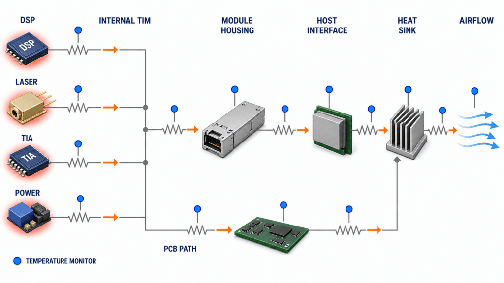
heat source → package or PCB → internal TIM → module housing or spreader → host interface → heat sink → airflow
Real modules also have parallel paths. Some heat spreads through the PCB. Some moves toward the connector. Nearby components can warm one another. The thermal model and test plan should reflect those branches instead of assigning all module power to one top-side interface.
Check the component-to-housing interface
Inside the module, the TIM may bridge a component or spreader to the upper housing. Record the physical gap at several points rather than relying on the nominal CAD value. Include component-height tolerance, housing flatness, PCB bow, adhesive layers, coatings, and support locations.
This interface often favors a conformable pad or dispensable gel because the surfaces do not start in direct contact. The correct choice depends on the working gap and the force that the assembly can accept.
Check the module-to-host interface
The external path has different demands. The module may slide under a riding heat sink, use an integrated heat sink, or contact another approved cooling surface. Flatness, roughness, normal force, heat spreading, insertion wear, labels, and surface treatments can all change contact resistance.
The OIF thermal interface agreement for pluggable optics treats these factors as part of the interface design. It also calls for application-specific consideration of module dissipation, local air temperature, air speed and direction, cage design, and nearby board temperature.
Do not add a soft TIM to a sliding module-to-host interface unless the mechanical system was designed and tested for it. Friction, wear, debris, and insertion force may become more important than the initial thermal result.
Find the largest temperature drop
A thermal-resistance budget helps locate the bottleneck. List the major segments between each heat source and the inlet air. Estimate or measure the temperature drop across the package, internal TIM, housing, host interface, heat sink, and airflow path.
If the main temperature rise occurs in the heat sink or airflow, a higher-conductivity pad inside the module may make little difference. If it occurs across a thick internal gap, changing the material, bond line, pressure, or contact area can have a much larger effect.
Match the material form to the interface
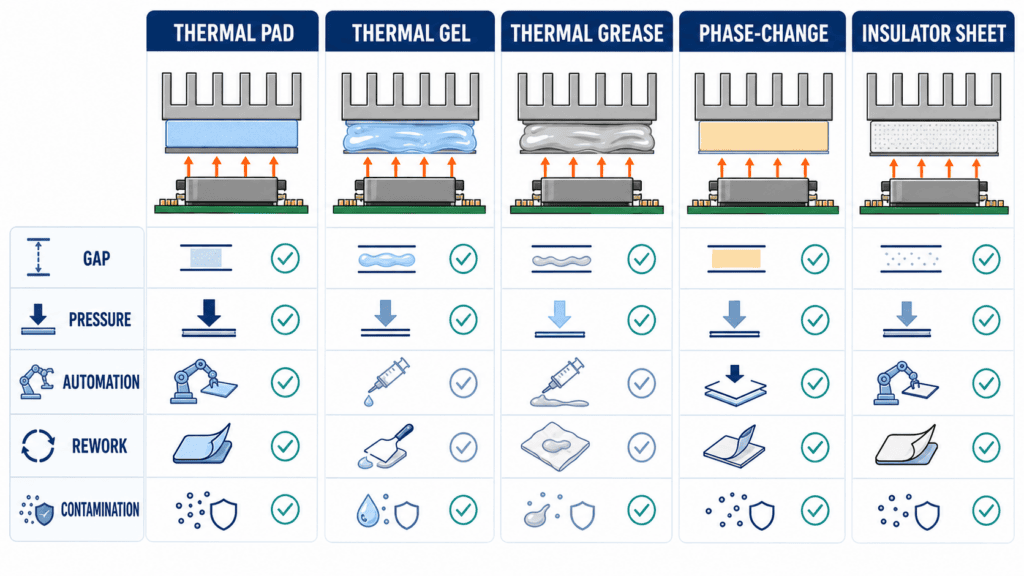
The material form determines how the interface fills a gap, transfers load, moves during temperature cycling, and fits the production process. Choose the form first. Compare conductivity after the candidates can perform the same mechanical job. Jiuju’s thermal conductive material overview shows the broader product families before the discussion moves to grade-level specifications.
| Material form | Where it can fit | Main issue to control |
|---|---|---|
| Thermal gap pad | Defined gap between a component, spreader, or housing | Compression force, missed contact, placement, and edge shift |
| Dispensable thermal gel | Irregular gaps or several component heights | Dispense volume, voids, overflow, pump-out, and rework |
| Thermal grease | Thin interface between surfaces that already approach each other | Migration, dry-out, pump-out, and process cleanliness |
| Phase-change material | Thin interface that wets after its designed transition | Activation, coverage, and temperature-process fit |
| Thermal insulator sheet | Interface that also needs a defined dielectric barrier | Damage, compressed thickness, and added thermal resistance |
| Graphite sheet | In-plane spreading from a local hotspot | Edge insulation, grounding, attachment, and through-plane contact |
Thermal pads for controlled gaps
A die-cut thermal pad is easy to place and inspect. It can accommodate flatness variation and provide electrical insulation when the selected grade and construction are qualified for that purpose. Pads work well when the gap is known and the assembly has enough force to create contact without damaging the board or package.
Jiuju’s current internal product matrix lists thermal pads from 1.2 to 25.0 W/m·K. The public thermal pad portfolio shows the main material categories, while the standard thermal pad specification table provides grade-level examples. Confirm the available grade and report during project review because thickness, hardness, compression force, reinforcement, electrical properties, and reliability still have to match the interface.
Thermal gels for uneven stacks
A dispensable gel can fill irregular gaps and several component heights with low initial assembly stress. It may also suit automated production when the dispensing window is properly controlled.
The process has to define bead position, dispense mass or volume, closure displacement, allowable overflow, and inspection method. A gel that looks acceptable before the lid closes may still trap a void or move into a keep-out area. Jiuju’s current internal product matrix lists thermal gels from 1.2 to 18.0 W/m·K. The working bond line and material state need grade-level confirmation; the public thermal gel portfolio outlines the main product forms.
Thin-interface materials
Grease and phase-change materials suit surfaces that already approach each other closely. They can form a thin interface, but they are not substitutes for a thick gap filler. Coverage, material movement, activation temperature, and rework all need to be considered in the actual assembly. The thermal grease product page is the relevant next step when the design already has a thin, controlled bond line.
Graphite, tape, and insulation
Graphite sheet spreads a local hotspot laterally. It does not fill a large uneven gap by itself. Thermal conductive tape can combine attachment and heat transfer where the bond line and long-term adhesion are controlled; Jiuju lists its available forms on the thermal conductive tape product page. An insulator sheet can add a defined dielectric barrier, but every extra layer adds thermal resistance.
These materials can work together. A graphite spreader may distribute heat before a pad transfers it to the housing. The design still needs a clear job for each layer. Adding materials without mapping the thermal path often makes the stack thicker and less predictable.
Six checks that determine installed TIM performance
1. Gap and working thickness
Measure the minimum and maximum assembled gap across several units. A pad must remain thick enough to contact the widest gap and soft enough to avoid excessive force in the narrowest gap.
For a pad with free thickness T and installed gap G:
Compression (%) = (T - G) / T × 100
Jiuju’s standard pad-thickness tolerance is generally reported as ±10%. A tighter ±5% tolerance can be discussed when the grade, construction, order quantity, and inspection agreement support it. Custom nominal thicknesses from 0.3 to 15 mm are available by project. Use the tolerance extremes in the stack calculation rather than treating the nominal thickness as exact. The thermal pad thickness selection guide explains the general measurement and compression method in more detail.
2. Pressure and total force
Compression percentage does not tell you the assembly load. Request the compression-deflection curve for the exact grade and thickness, then convert pressure into total force:
Force = pressure × contact area
A large pad can create substantial force even at a moderate pressure. Check PCB bow, housing deformation, fastener seating, package load, and optical alignment. A softer material can reduce stress, but it still needs enough pressure to wet both surfaces.
3. Installed thermal impedance
Bulk conductivity is only one part of the installed result. Thickness and contact resistance also matter. A lower-conductivity material can outperform a higher-conductivity option if it forms a thinner, more complete interface at the available pressure.
ASTM D5470 provides a method for comparing thermal transmission properties of TIM specimens. Compare candidates at similar thickness, pressure, temperature, and construction. Then confirm the result in the module because a laboratory fixture does not reproduce the complete mechanical stack.
4. Electrical requirements
Do not infer insulation from color or polymer family. Verify volume resistivity, breakdown behavior, reinforcement, compressed thickness, creepage, and clearance for the selected grade. Include placement tolerance and edge extrusion near exposed conductors. If the module also has an electromagnetic compatibility problem, review it as a separate requirement against Jiuju’s EMI shielding and absorbing material options rather than assuming the thermal material will solve both jobs.
5. Optical cleanliness and material movement
Check volatile loss, oil bleed, condensable species, pump-out, and compatibility with nearby coatings, lenses, connectors, and PCB surfaces. Material chemistry alone does not predict whether an optical surface will remain clean.
6. Assembly and rework
The drawing should control pad outline, liner orientation, placement, and compression. A gel process should control cartridge handling, purge, dispense quantity, bead continuity, closure, and overflow. The best material is one production can apply, inspect, and repeat.
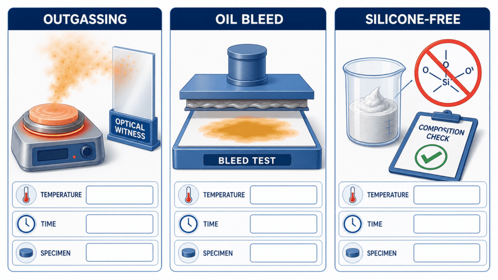
Low outgassing, low bleed, and silicone-free mean different things
These terms are often grouped together, but they answer different questions:
- Low outgassing describes material loss or released species under a defined test condition.
- Low bleed describes liquid-phase migration into an adjacent surface or test medium.
- Silicone-free describes material composition. It does not prove zero volatility or zero contamination.
The risk depends on temperature, time, exposed area, distance to the optical surface, airflow, enclosure volume, and material compatibility. A general mass-loss value cannot predict lens haze by itself. A paper-bleed test cannot identify every condensable species.
The Sandia survey of thermal interface materials treated thermal aging, optical and chemical change, and offgassing as separate measurements. An optical-module program should do the same. Pair material screening with an assembly-level test using witness coupons or the relevant optical surface. Record the temperature, time, enclosure condition, specimen geometry, and acceptance limit.
Jiuju reports a non-silicone F6000 pad family covering 1.2 to 8.0 W/m·K. Internal product data reports volatile mass loss no greater than 0.5% after 120°C for 72 hours for that family. Keep the test condition and product family attached to the value. Confirm the report for the selected grade before using it in a project specification. The low-bleed and non-silicone categories can be reviewed in the broader thermal pad product range.
How module architecture changes the material decision
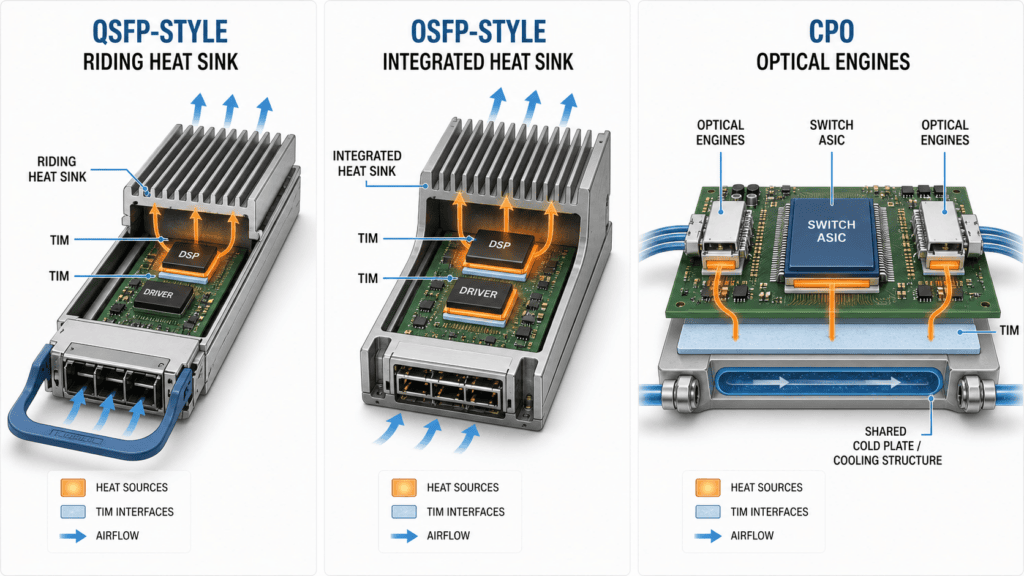
SFP, QSFP, QSFP-DD, and OSFP modules do not share one force budget or heat-sink geometry. Modules in the same form factor can also differ in reach, DSP architecture, optical engine, housing construction, and power state.
An integrated heat sink places part of the cooling structure on the module. A riding heat sink transfers load from the host onto a defined module surface. Each arrangement changes the contact area, flatness requirement, insertion behavior, and path to the airflow. Use the applicable mechanical specification and module data before selecting an interface treatment.
Co-packaged optics changes the design more substantially. Optical engines sit close to a switch ASIC or another high-power device, and several heat sources may share a cold plate or other cooling structure. The optical engine and ASIC can have different temperature and mechanical limits. A TIM stack developed for a pluggable module should not be scaled down and reused without a new thermal network, tolerance study, cleanliness review, and service plan.
A practical TIM selection workflow
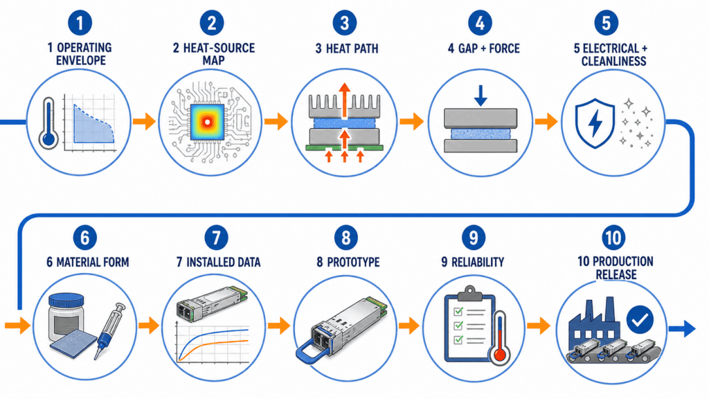
- Define the operating envelope: module dissipation, power states, inlet temperature, airflow, orientation, environment, and life target.
- Map the heat sources: component power, contact area, temperature limit, and available monitor points.
- Draw the full heat path through the package, PCB, internal TIM, housing, host interface, heat sink, and airflow.
- Measure the mechanical stack at several locations and across several units. Include flatness, roughness, supports, and deformation limits.
- Set the electrical and cleanliness requirements, including insulation, keep-out areas, volatile behavior, bleed, and compatibility.
- Choose the material form by interface function before comparing grades.
- Compare installed data at the intended thickness, pressure, and temperature.
- Build multiple prototypes and inspect contact, seating, force, temperature, cleanliness, and process repeatability.
- Run reliability tests that represent the actual risks, then repeat the thermal, optical, electrical, and mechanical checks.
- Release the material and process together, including grade, thickness or dispense target, tolerance, placement, inspection, traceability, and reaction plan.
Validate the material in the assembled module
Coupon data is useful for comparing materials. It does not release the module. Validation should move through four levels:
- Material inspection checks thickness, hardness or viscosity, thermal data, electrical properties, and the agreed cleanliness indicators.
- Subassembly inspection checks contact print, bond line, voids, overflow, placement, and deformation.
- Module testing checks internal and case temperature, optical performance, power-state response, and sensitivity to airflow.
- Reliability testing checks whether the interface moves, cracks, bleeds, loses contact, changes electrically, or contaminates nearby surfaces after exposure.
Jiuju’s documented test capability includes thickness, hardness, compression, electrical testing, ASTM D5470 thermal testing, high and low temperature exposure, damp heat, thermal cycling or shock, volatility, and oil-bleed evaluation. The relevant tests, conditions, sample quantity, and acceptance limits must be agreed for the selected material and project.
Shipment reports also need to match the material form. Pad documentation can include conductivity, hardness, dimensions, appearance, and agreed project checks. Gel documentation may use viscosity, extrusion output, or cured hardness instead. A useful quality agreement defines the method, frequency, limit, and response to an out-of-control result.
Jiuju’s documented project workflow uses APQP, DFMEA/PFMEA, ERP/PLM document control, and an issue-evaluation/8D loop. For an optical-module program, this workflow keeps the approved grade, die-cut drawing or dispense target, inspection method, and change history in one release package.
Frequently asked questions
What is the best TIM for an optical transceiver?
There is no universal best material. A pad can suit a controlled gap, while gel may suit irregular component heights. Grease or phase-change material may fit a thin interface. The selected material has to meet thermal, mechanical, electrical, cleanliness, process, and reliability requirements in the same assembly. Jiuju’s TIM form-selection guide provides a broader comparison of pads, fillers, and gels.
Does an 800G or 1.6T module always need a higher-conductivity pad?
No. Data rate does not define the complete heat load, hotspot area, gap, contact pressure, housing, heat sink, or airflow. Start with the actual module and host design, then compare materials at the installed thickness and pressure.
Should every optical module use a silicone-free TIM?
No. Use the project’s contamination rules and test evidence. Silicone-free chemistry may be required in some optical environments, but it does not automatically prove low outgassing, low bleed, or long-term stability.
Is module case temperature enough for validation?
Not always. An internal DSP, laser, TIA, or power component may have less margin than the case. Use supplier-defined monitor points where available and correlate them with the case and host conditions.
What should be sent to a TIM supplier?
Send an anonymized cross-section, heat-source map, power states, contact area, gap range, force limit, electrical requirements, cleanliness requirements, environmental conditions, assembly method, and acceptance criteria. These inputs allow the supplier to compare material forms and prepare a useful sample plan.
Build the cooling solution around the actual interface
Optical module cooling depends on the complete path from the heat source to the inlet air. A high conductivity number cannot fix a missing contact area, an overloaded package, a weak heat sink, or contamination beside an optical surface.
Start with the heat map and mechanical stack. Choose the material form for the interface, then compare grade-level data at the intended thickness and pressure. Validate thermal performance, force, electrical behavior, cleanliness, and production control in the assembled module.
For a new project, review Jiuju’s thermal material capabilities, the thermal pad specifications, and the thermal gel options. Send the anonymized module inputs listed above through the Jiuju contact page. The team can use them to prepare a material shortlist, die-cut or dispensing recommendation, and a project-specific validation plan.
Effective